|
This document describes the design and building of a Universal HF Receiver
Last Updated Tue, 13 Jul 2021 17:11:12 -0400 Always check the Addendum Section for updates before starting the kit build. |
Build this Universal Receiver for $20
Plus Band Kits for $10 each
|
Click to View Operational Prototype in new window
Click to View "Band Parts Table (ODS)" in new window
Click to View "Band Parts Table (HTML)" in new window
Universal Receiver VCXO Band Kit Instructions for 10M 12M 15M 17M 20M 30M 40M 80M 160M
Universal Receiver VFO Band Kit Instructions for 10M 12M 15M 17M 20M 30M 40M 80M 160M
Universal Receiver DDS Instructions
Mute Kit Instructions
Click to View "Theory of Operation" in new window
Base Kit Building Instructions:
DO NOT REMOVE ANY PARTS FROM THE PLASTIC BAGS UNTIL INSTRUCTED TO DO SO
Parts List
Do not mix up the red 1N4148 signal diodes with the red 1N5240B zener diode.
If you are missing any parts, contact me immediately. I will ship the parts the same day.
If you find extra parts in the kit, check the Addendum else throw them in your junk box.
This kit comes in 3 parts: Basic Receiver Kit, Band Kit and Mute Control Kit.
The Basic Receiver Kit and Band Kit contain all parts to create a fully functioning HF receiver.
Included parts are: 1 phone jack, a bnc jack, volume and tune controls and magnet wire.
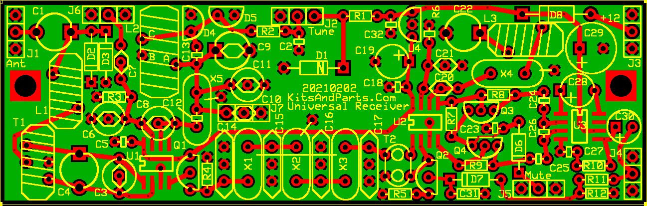
Install the parts in the order per this document to prevent mechanical installation problems later.
This kit requires the following items to complete the kit:
Hook-up wire #22 or #24 gauge to connect the PCB to the controls and enclosure.
Rosin Solder 60/40 (OK) or 63/37 (Best) and a fine tip temperature controlled solder pencil.
Tool for adjusting trimmer capacitors - suggest search for GC-8608
Optional freq counter type PLJ-0802 - search ebay 261731946045
Manual for PLJ-0802 Frequency Counter
Optional power on/off switch.
Optional Case - Suggested Cases
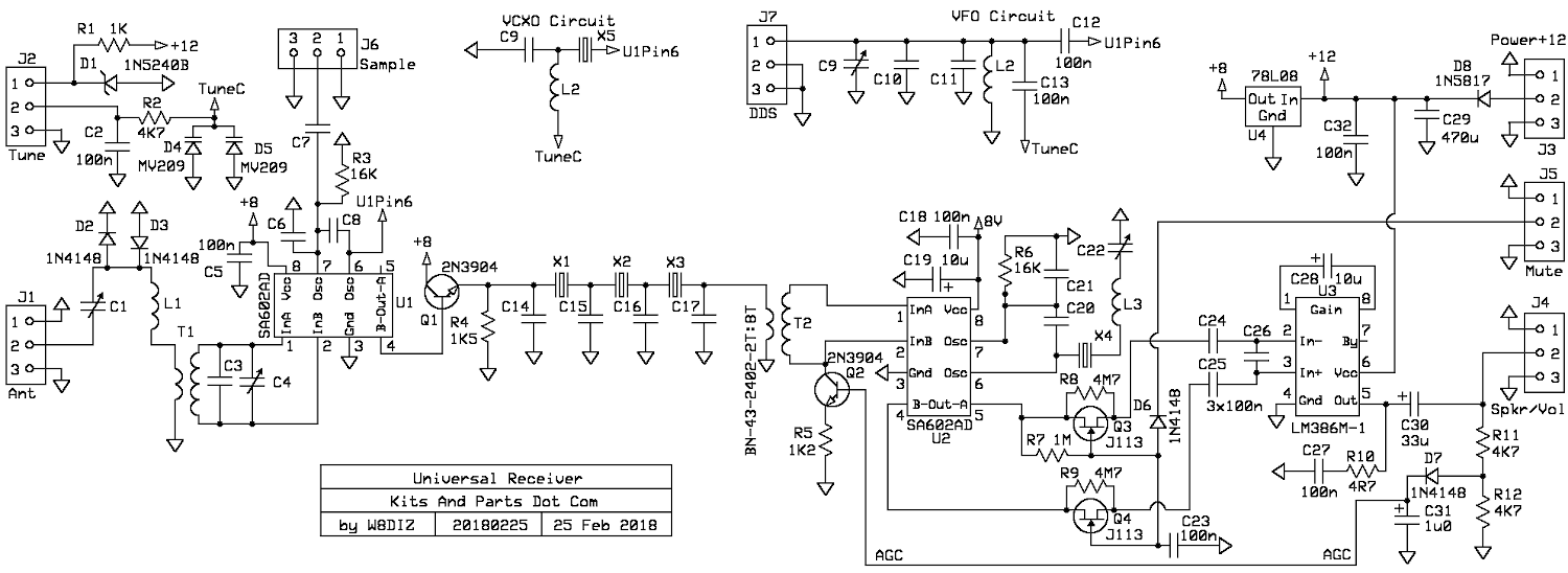
1. Install all three (3) SMT ICs observing correct orientation
____U1: SA602AD First Mixer IC
____U2: SA602AD Second Mixer/BFO IC
____U3: LM386-M1 Audio Amplifier IC
2. Install all 100n (0.1uF) green 2.5mm spacing capacitors EXCEPT C12 & C13
____C2,5,18,24,25,26,27,32
3. Install all 1/8 Watt Resistors EXCEPT R3 & R6 & R12
See NE602A spec sheet page 6 for more information about the internal oscillator DC bias current
If you must install R6, note that it is installed vertical.
R12 is included in the MUTING Kit.
You may need a magnifying device to verify the resistor color codes.
Bend the resistor leads a sharp 90 degrees from the body of the resistors.
R13 and R14, the volume control and tune control will be connected later.
Save 6 cut resistor leads to ground the crystal cases later and other needs.
____R1: 1K Brown-Black-Red-Gold
____R2,11: 4K7 (4.7K) Yellow-Violet-Red-Gold
____R4: 1K5 (1.5K) Brown-Green-Red-Gold
____R5: 1K2 (1.2K) Brown-Red-Red-Gold
____R10: 4R7 (4.7) Yellow-Violet-Gold-Gold
4. Install three (3) Yellow Trimmer Capacitors
____C1,4,22 (optional C9 is Customer Supplied)
5. Install all Diodes observing correct orientation
____D1: 1N5240B Red 10 V Zener
____D7: 1N4148 Red Signal Diode
____D8: 1N5817 Black rectifier Diode
____D4: MV209 Varactor Diode TO-92 (install 1/8 inch above the PCB floor)
____D5: Varactor Diode - user supplied optional part for experimenting
6. Install transformer T2
Cut 10" of #34 red wire and 4" of #30 red wire.
____T2: Wind 8 turns of #34 red wire on an BN-43-2402 black ferrite binocular.


Trim the red wires of T2 to one inch each.
Wind 2 turns of #30 red wire on the BN-43-2402 black ferrite binocular.
Trim the #30 wires of T2 to one half inch each.
Strip & Tin the insulation on all 4 wires to the base of the binocular.
The #34 wire leads for the 8 Turn winding go to the two pads towards Q2.
The #30 wire leads for the 2 Turn winding go to the two pads towards C17.
Install T2 into the PCB, pull the leads tight using needle nose pliers, solder and trim.
7. Install Transistors and the voltage regulator observing correct orientation
____Q1: 2N3904 NPN Transistor
____Q2: 2N3904 NPN Transistor
____U4: 78L08 Voltage Regulator 8 volts
8. Install all remaining Capacitors observing polarity orientation
____C7: 4p7 or 10pF NPO Disc
____C19,28: 10 uF Electrolytic
____C29: 470 uF Electrolytic
____C30: 33 uF Electrolytic
____C31: 1u0 uF (105) Yellow Cap
9. Install 2 jumpers if not using the MUTE KIT
____Jumper1: Use a cut resistor lead and install the jumper across R8
____Jumper2: Use a cut resistor lead and install the jumper across R9
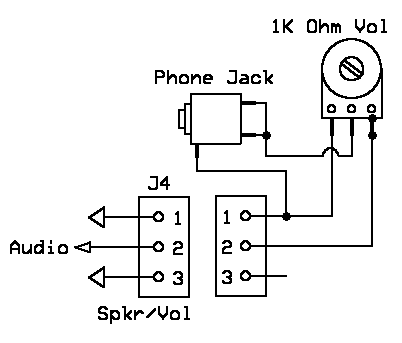
10. Install Volume Control
____Connect the volume control as show:
Notes:
Documentation on International Radio Frequency Bands (0-30 MHz)
| Variable capacitor settings | |||||
|---|---|---|---|---|---|
| Maximum Capacitance | Midway Capacitance | Minimum Capacitance | |||
 |  |  | |||
If you need an alignment tool for the trimmer caps,
look up "GC 8608" - available at newark.com and onlinecomponents.com
Addendum Section:
March 14 2018 - On the PCB, D1 near J3 should be labeled D8 per the schematic.
March 29 2018 - On the PCB, C25 next to C29 should be labeled C28 per the schematic.
End of Addendum Section: top