The Universal Receiver was designed for kitbuilders to create a simple but functional receiver for any frequency from below the AM Broadcast Band up to the 10 meter Ham band.
Any and all suggestions and edits to improve this document are very welcome and anticipated.
Contact Link
Universal Receiver - Theory of Operation
Below example is for a 40 meter receiver.
Power
Power to the receiver should be a AC/DC Power Supply or 12 volt Gel-Cel Battery. Voltage source should not exceed 15 volts.
Power is connected via J3, a standard 0.1 inch 3 pin header or direct soldered wires. J3 Pin 2 is plus 12V; Pins 1&3 are ground.
Voltage reversal protection is provided by D8, a 1N5817 Schottky diode with a typical 0.3 or less volt drop when the receiver operates normal.
The 12 volts is supplied directly to the LM386-M1 Audio Amplifier which has a maximum volatage reating of 15 volts.
The 12 volts is also connected to a 10 volt Zener Diode D1, a 1N5240B which provides the source of the Varactor (D4,D5) tune voltage.
12 volts is also the source for the 8 volt TO-92 regulator U4, a 78L08 which provides power to the two SA602AD balanced mixers, U1 & U2.
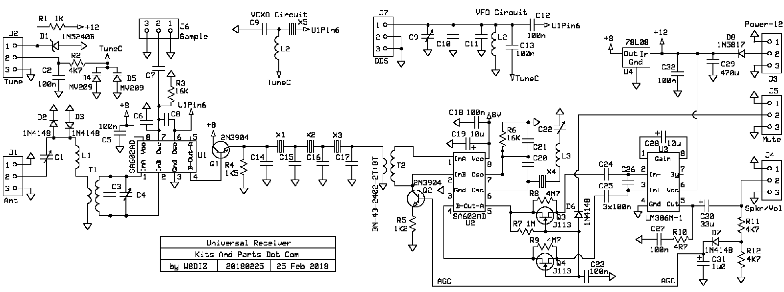
Antenna Connection - RF Input Circuit
The input circuit to the first mixer consists of 2 sections; C1-L1 and T1-C3-C4
C1-L1 is a series tuned circuit at the frequency of interest. The inductive and capacitive reactances of C1 & L1 should be as high as practically possible.
When a high level (like a transmitter) 50 ohms antenna signal is passed though the series tuned circuit, the voltage at the junction of L1-C1 will be very high
relative to the input and output of the L1-C1 circuit. Two silicon signal diodes are placed at the junction of L1-C1.
These diodes will conduct when a high level signal is present at the antenna input but will not conduct with low level antenna pickup signals,
providing input protection to U1, the first mixer.
T1-C3-C4 is the main band pass filter for the receiver. The in/out turns ratio of T1 is calculated based on 50 ohm source and 3000 ohm balanced input to U1.
The ratio (3000/50) is 60. The turns ratio should be the square root of 60 which is 7.75 so the wire turns ratio of T1 should be 7:1 or 8:1
Using a turns ration of 4 turns primary (from antenna) and 30 turns secondary (to mixer) and C3=100pF and C4=45pF timmer, we have a 40 meter bandpass circuit.
A link that provides design assistance for the T1 bandpass circuit can be found at toroids.info
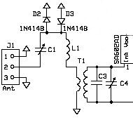
First Mixer - The SA602AD mixer is capable of receiving -119dBm signals with a 12 dB S/N ratio.
The SA602A mixer is commonly powered with 6 volts with a maximum rating of 9 volts. It is operated here at 8 volts for improved performance.
The rf input circuit connects to the 3000 ohm balanced input of the first mixer (U1) on pins 1 & 2.
Voltage measurements for pins 1 & 2 are about 1v43. Voltage measurements for the output pins 4 & 5 of U1 are about 6v8.
The SA602A internal oscillator transistor is biased with only 220 uA. In order to assure oscillation in some configurations, it may be necessary to increase
transconductance with an external resistor (R3) from the emitter to ground. 10K to 22K are acceptable values. We use a 16K resistor, only when required.
C6 and C8 provide the external feedback network for the internal oscillator. Published formula for calculating C8 is 100/sqrt(F) and C6 is 1000/F, where F is
the frequency in MHz and the result of the calculation is in pF. At HF frequencies, the ratio of C6/C8 is about 2:1 or 3:1 but have seen 1:1 in many designs.
C7 is the coupling capacitor to the header J6, which is used to connect to a frequency counter such as this one found on Ebay.
The value of C7 should be as small as possible while still providing a stable freq readout. Typical values are 4p7 or 10pF; larger values for lower frequencies.
The First Mixer is configured to provide the oscillator signal in one of three ways: VCXO, VFO or DDS. Details follow below.
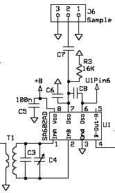
VCXO Circuit (Voltage Controlled Crystal Oscillator)
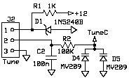
The VCXO consists of a voltage controlled Varactor Diode MV209, a Crystal (X5) and an Inductor (L2).
For the VCXO, capacitors C10,11,12 and 13 are not installed.
The Tuning Voltage is supplied to the Varactor from a 10 volt Zener Diode (D1) 1N5240B through a 100K (R2) isolation resistor. The value of R2 may be
reduced (lowers the Q of the Varactor) in some cases if the VCXO is not perfectly stable due to circuit design restrictions.
A small (3-10 pF) capacitor C9 may optionally be installed. This capacitor causes the frequency span to increase by lowering the low frequency end of the VCXO.
Example: A 23.04 MHz VCXO oscillates from 23.24 to 23.039; a freq span of 15 KHz.
By adding a 10 pF cap at C9, the 23.04 MHz VCXO oscillates from 23.12 to 23.038; a freq span of 26 KHz. Bigger is usually better.
Adding too much capacitance at C9 may make the VCXO unstable on part or all of the tuning range.
The higher the inductance of L2, the less capacitance at C9 is required for C9 to have an effect on the tuning range.
To create the widest frequency span of the VCXO, the inductace of L2 should be the highest possible while making sure the VCXO is stable at both ends of the tune range.
If you find that the tuning at one end of the tune range becomes unstable, reduce the turns on L2.
VFO Circuit (Variable Frequency Oscillator)
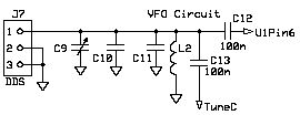
The VFO consists of a voltage controlled Varactor Diode MV209, capacitors C9,10,11 and an Inductor L2.
C12 isolates Pin 6 of the Mixer (U1) from ground via L2. C13 isolates the tune varactor voltage from ground via L2.
C9 is optioally an NPO trimmer cap. The caps C10 and C11 should be NPO or C0G or Polystyrene.
For HF VFO designs, L2 is most often a T68-7 Toroid because of it's lowest temperature coefficient. They have a Temperature Stability of 30 ppm /°C.
Type -6 material toroids have a Temperature Stability of 35 ppm /°C and Type -2 material toroids have a Temperature Stability of 95 ppm /°C.
DDS Circuit (Direct Digital Synthesis)
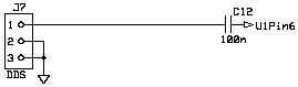
The DDS signal source must be applied to the mixer U1 via J7 coupled through C12 (provides DC voltage isolation).
The DDS signal amplitude should be about 700 millivolts P-P for optimal mixer signal conversion.
Components C9,10,11,13 and L2 and X5 are not installed. Additionally, the tuning voltage circuit comprised of R1, D1, C2, R2, D4 and D5 are not required.
Crystal Filter
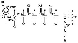
The crystal filter was designed using Advanced Empirical Methods Technology (AEMT)
Another definition of AEMT is guessing what should be suitable component values, then testing the circuit.
Q1 is a Emitter Follower Amplifier; it amplifies the mixer out signal and helps match the 1500 ohm output of U1 pin5 to the crystal filter.
Voltage measurement at the Emitter of Q1 is about 6v1.
The Crystal Filter (for 7 MHz Receiver) uses 16 MHz crystals. Load capacitors (C14-C17) for narrow band CW operation should be about 680pF.
Crystal Filters that uses 10 MHz or lower freq crystals may use 470pF load capacitors (C14-C17) for narrow band CW operation.
For SSB or wide band filters, C14-C17 should be 100 pF or less.
All crystals cases should be grounded to prevent pickup of stray RF signals.
T2 is a transformer using a 1:4 turns ratio that matched the output of the filter (100-500 ohms) to the balanced input impedance (3000 ohms) of the 2nd mixer U2.
Second Mixer/BFO
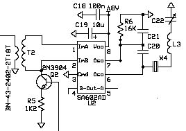
The SA602A BFO is commonly powered with 6 volts with a maximum rating of 9 volts. It is operated here at 8 volts for improved performance.
The rf input circuit connects to the 3000 ohm balanced input of the first mixer (U1) on pins 1 & 2.
Voltage measurements for pins 1 & 2 are about 1v43. Voltage measurements for pins 4 & 5 of U2 should be near 6V2 with antenna disconnected
and near 8V0 with antenna connected and receiving a loud/strong signal.
The SA602A internal oscillator transistor is biased with only 220 uA. In order to assure oscillation in some configurations, it may be necessary to increase
transconductance with an external resistor (R6) from the emitter to ground. 10K to 22K are acceptable values. We use a 16K resistor, only when required.
C20 and C21 provide the external feedback network for the internal oscillator. Published formula for calculating C8 is 100/sqrt(F) and C6 is 1000/F, where F is
the frequency in MHz and the result of the calculation is in pF. At HF frequencies, the ratio of C21/C20 is about 2:1 or 3:1 but have seen 1:1 in many designs.
The value of L3 is such that you can adjust C22 to obtain the correct BFO offset frequency, usually 600 Hz from the crystal filter center frequency.
Also connected to the input is the Collector of the AGC amplifier Q2.
Audio Amplifier LM386-M1
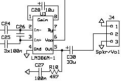
The LM386 audio circuit is a standard design, configured for maximum gain with the 10uF cap C28.
C27 and R10 compose a "Boucherot cell" which prevents audio oscillations at very high volume.
Mute Circuit
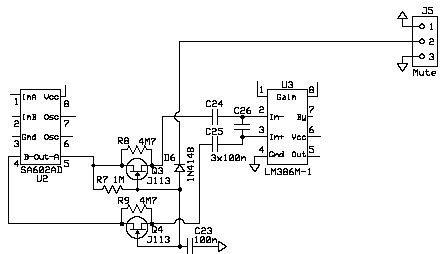
The mute circuit is controlled by an external control circuit. Grounding pin 2 of J5 enables audio muting.
Fets Q3 and Q4 are turned on when pin 2 of J5 is open. This allows the Source and Gate of the Fets to be at the same potential and conduct.
Grounding pin 2 of J5 will ground both Fet gates, turning off the Fets.
The RC Time Constant of R7 and C23 determine the QSK delay from muting to reveive mode.
R8 and R9 are installed to enable "natural sidetone" when using a common VFO/DDS for transmit and receive.
They should not be installed if the receiver and Transmitter use independent tune sources
AGC
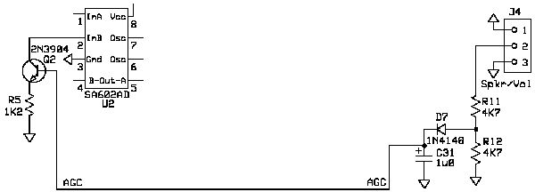
The AGC control voltage is created by sampling the audio from J4. The audio is limited by R11 4K7 and then rectified and filterd by D7 and C31.
The AGC control voltage then controls the conduction of Q2. The more Q2 conducts, the lower the voltage on pins 1 & 2 of U2, reducing U2's gain.
Finis