Kit only $9!
(Assembled, tested and calibrated for $25 - limited availability)

This is not a beginner-level kit. You should have some confidence in soldering SMD devices
(including 0805 size components and the 10-MSOP package of the Si5351)
and you should have access to hot-air SMD soldering equipment or a reflow oven/hotplate.
With that said, this is a fairly simple kit with only 13 components to install.
What is it?
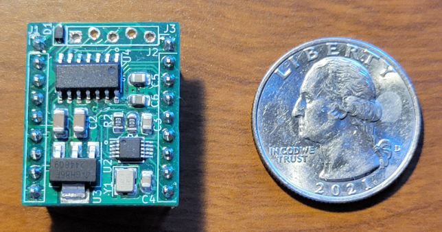
The Uni-VFO is a compact (21mm x 25.4mm) (0.83” x 1”) synthesized VFO kit for experimenters.
The purpose of this kit is to provide a simple, inexpensive, small and field-configurable VFO.
The output can be a single clock or a pair of quadrature clocks for the VFO, along with a
2nd static clock that can be used as a BFO in a superhet receiver.
Why is it different?
A departure from the “standard” Si5351 VFO, there is no display, no encoder and no switches.
Tuning is accomplished by a single potentiometer (not included in the kit), simulating the
old-school smoothness of an analog VFO. Tuning boundaries are configured in advance,
and those settings define the VFO frequencies from low to high as you turn the tuning pot.
Since the tuning is “absolute” (relating to the actual position of the pot),
saving a startup frequency is not necessary.
You pick up where you left off when you power it back on, just like the old days. :)
How does it work?
Connect power (5.0V - 15VDC) to Vin and Gnd, and a potentiometer of your choice
between 3.3V and Gnd, with the wiper on Vtune.
Configure desired frequencies via your PC's serial port.
Connect the clock outputs to your circuits. Tune your Uni-VFO with the potentiometer.
The position of the potentiometer is converted to a 12 bit number, then the output frequency is set accordingly.
Easy-Peasy
Here's a quick video of the Uni-VFO in action, driving the K7QO DC receiver (you qrp-tech folks will remember that project).
Notice the smoothness of the tuning across the CW portion of 40 meters.
Link: Demo Video
What do you need?
This kit, a linear potentiometer (<10k recommended), SMD soldering tools, a USB-TTL serial converter and, of course, a circuit that needs a VFO.
Schematic
Board Images


Parts List
|
Build Instructions
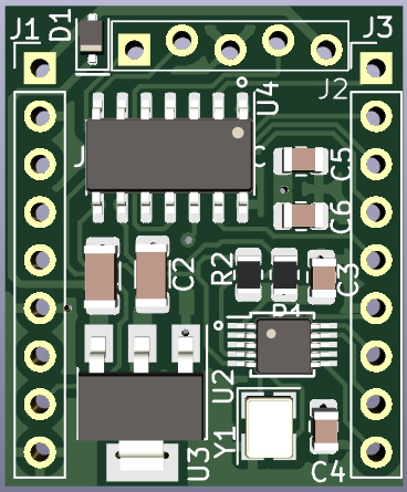
Install the Si5351 and the Microcontroller first. Note the dot on the PCB that denotes pin 1.
Install the reverse polarity protection diode, D1.
Note the band on the diode D1 is away from the edge of the board. The cathode mark on the PCB is hard to see.
This part is difficult to solder since the solder pads are so small, and because the part can fall over.
Be careful.
Install the regulator, U3. Make sure you solder the tab as well as the three pins.
Install the 25MHz crystal Y1. Note that it is oblong, not square. Notice the marks on the PCB.
It can be installed properly in two positions, 180 degrees rotated. Check the board picture above.
Install the two 10k resistors in positions R1 and R2
Install the capacitors. Notice that C1 and C2 are larger (1206 package). C6 is the single unmarked cap.
There is one spare 0.1uF capacitor included. If necessary, it can be used as a filter cap between the
VTune pin and ground.
Install the two 9 pin header strips (if desired) in J1 and J3.
The 5 pin programming header is usually not installed permanently. See "Configuration" section below.
Programming
Programming the microcontroller is not necessary since KitsAndParts will pre-program
the microcontroller with the latest code before shipping.
Pinout
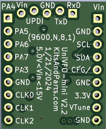
The signals are brought out in two 9 pin, 0.1" (2.54mm) spacing PCB pads, exactly 0.7" apart.
You can solder header pins (included) and plug this directly into a proto-board,
or solder to another PCB of your design. You can also simply hard-wire it in place and skip the connectors.
Vin - Input DC voltage from 5.0V to 15V (reverse polarity protected)
Gnd - Ground pins
SCL / SDA - Microcontroller's I2C lines. These are 3.3V only!
3.3V - output of the Uni-VFO 3.3V linear regulator. This can supply quite a bit of extra current, but be aware of the increased power dissipation in the regulator.
VTune - From the wiper of the tuning pot. This voltage is translated into the VFO frequency as you tune.
CLK0 / CLK1 / CLK2 - These are the direct output clocks from the Si5351
PA3 / PA4 / PA5 / PA6 / PA7 - Extra unused GPIO from the ATTiny3224
Configuration
Configuration is done via a simple serial port connection to a computer,
using a terminal program like "PuTTY" for Windows (or Minicom for Linux) at 9600bps.
Configuration and programming are done via a separate 5 pin connector on the PCB.
To save cost and space, the pads are slightly offset in a zig-zag pattern.
This allows the use of a 5 pin header strip to connect the signals, and the zig-zag pattern creates a
friction fit into the holes. You can easily, temporarily connect to this for programming or configuration,
then remove it when installing into your radio. You can also solder a connector here if you desire a more permanent connection.
The RxD and TxD pins on the Uni-VFO require TTL level serial connection to your PC.
The easiest way to do this is to use a USB-TTL adapter (also available from KitsAndParts.com)
Plug the adapter into a USB port on your computer and see what serial port number (i.e. Com4) it is assigned
by looking in Device Manager (for windows). The example below shows the adapter connected as COM4.
Start PuTTY and select "Serial" for connection type.
Enter the serial port number in the "Host Name" field (in this case, COM4), then click "Open". You'll get a black window.
Connect the Rx/Tx pins from the PC's USB-TTL adapter. In order to communicate, the signals are crossed,
so RxD from the serial adapter goes to TxD on the Uni-VFO, and vice-versa. Also connect a ground between them.
Short the CFG/ pin to ground before powering up the VFO, then connect power to the Uni-VFO.
The board starts in configuration mode and generates a menu on the terminal,
where you can set frequency boundaries, change output types, enable or disable the BFO, and calibrate the PLL.
When the board is first started, it loads defaults from the firmware into EEPROM. Run through the menu to set the desired configuration.
The displayed menu shows the currently saved configuration, along with menu choices to modify it.
After each menu item is completed, the changes are saved to EEPROM and will take effect on restart.
When the configuration is done, disconnect the TxD and RxD lines, and remove the ground from the CFG/ pin.
You can now use the VFO in your circuit.
Note: If there is a problem communicating with the Si5351, the 2nd line will say "Si5351 missing" and the program will halt.
The remainder of the menu will not display.
Check the soldering around the Si5351, and anything connected to the I2C lines and try again.
Menu Descriptions
Calibrate PLL - Allows improved accuracy by compensating for differences in the 25MHz crystal.
A 10MHz signal is sent to CLK0. Adjust to exactly 10MHz using a frequency counter, or zero-beat WWV.
Use the keyboard to adjust the reference frequency
press a=+100Hz, z=-100Hz, s=+10Hz, x=-10Hz, d=+1Hz, c=-1Hz
press 'q' to stop the calibration routine and save the latest value.
As the frequency is adjusted, the compensated 25MHz reference clock values are displayed.
Set Start Frequency - This is the lowest frequency that will be created with the tuning pot completely CCW.
This menu entry also allows you to configure the Clk0 output as "locked", if you want a fixed frequency output,
and also allows you to configure the tuning knob for reverse operation (useful in some Superhet receivers)
The minimum output frequency in non-quadrature mode is 500kHz.
Set Step Size - The resolution of the ADC is 4096. This value is the number of Hz the VFO will change per ADC count.
A value of 10 will give a tuning range of 40960Hz.
Enable BFO - Turns on the BFO signal on CLK2. Enter the desired BFO frequency in Hz.
Calibrate BFO - This allows you to move the BFO +/- 2048Hz to find the center of your crystal filter.
In this mode, the BFO will be adjusted by turning the tuning knob. Clk0 is fixed at the vfo start frequency.
If you don't know the exact center of your fiter, you can find the peak (measure with an AC voltmeter or on an oscilloscope).
When you quit, it will save the adjusted value as your BFO.
Set Quadrature Mode - Enables 90 degree quadrature clock generation on CLK0 and CLK1. There is a lower limit on clock frequency in this mode.
The Si5351's internal Feedback Multisynth normally runs between 600MHz and 900MHz. In that range, the minimum VFO frequency in quadrature mode is 4.2MHz.
The PLL Multisynth can be run outside its normal range to provide quadrature outputs down to 3.2MHz.
Enable PLL Underclock (see below) to allow these lower frequencies.
Set Debug Mode - Debug mode dumps the Si5351 registers, as well as outputting the raw ADC tune values to the terminal
There is a slight delay between frequency changes in Debug mode, since the system has to wait
for the frequency to be displayed on the terminal before it continues. It is suggested
to only run in debug mode during debugging (Duh!).
Enable PLL Underclock - Allows the system to run the PLL clocks below the rated frequencies,
(down to 400MHz) which then allows lower quadrature VFO clocks down to 3.2MHz.
This does run the Si5351 out-of-spec, but is commonly done to cover 80 meters. Enable this only if needed.
Set clock output power - Sets the drive current for each clock (2mA, 4mA, 6mA or 8mA)
Show Current Config - prints the current config to the terminal
Additional Information
KitsAndParts also carries the required USB-TTL adapter, and a UPDI programmer for those who want to tinker with the software.
Link: USB-TTL adapter
Link: UPDI Programmer
The Clk0, Clk1 and Clk2 outputs are approximately 3.3V square waves that come directly from the Si5351.
There is no additional buffering on the VFO.
Some circuits may require a buffer to drive their load properly (like a MOSFET transmitter, for example).
You should keep the line lengths as short as possible. This includes the TTL serial lines.
An electrically noisy environment can cause incorrect characters to display on the terminal during configuration.
In an electrically noisy environment, you may see the VFO jump up or down one count from the noise on the ADC input.
(The raw ADC values can be viewed on the terminal when the Uni-VFO is in Debug mode)
If this happens, we included an extra 0.1uF chip capacitor that you can solder between VTune and ground to filter noise.
Also, lower resistance value tuning potentiometers are less susceptible to noise. We suggest chosing a pot that is less than 10k ohms (linear taper).
(Although I used a 10k linear pot during my testing without any issues)
If you are shy about soldering the MSOP-10 package of the Si5351, you can chose to leave it off the board, along with the 25MHz crystal.
You can then connect one of the Adafruit Si5351 breakout boards (or other Si5351 breakout board) to the Uni-VFO
SCL, SDA, 3.3V and Ground lines. It will operate the breakout board correctly when connected like this.
The control code is not open-source, but bug fixes and enhancements will be made available with a HEX file
that can be loaded by the user. Updates will be provided at no cost.
The Microcontroller is not locked, so any code can be run on it, and the original code can be returned if desired.
Accordingly, this code will run on non-KitsAndParts hardware, if desired (although we appreciate you buying our kits).
The Si5351 (or MS5351) frequency generator is controlled by a Microchip ATTiny3224 microcontroller.
This has 32k Bytes of program memory, 3k Bytes of static RAM and 256 Bytes of EEPROM
(all equal to or better than the specs of an Arduino Nano). The control code from KitsAndParts is
written in C and compiled with the Microchip Studio development environment.
Using plugins, you can write your own code for this in the Arduino environment too (see programming notes below).
Link: megaTinyCore
Link: Example Blink Sketch
Link: Simple VFO Demo Sketch
This module was purposefully designed to allow maximum flexibility when used in new designs.
All microcontroller signals are brought out to header-pins, including the I2C SCL and SDA (3.3V level)
if you choose to connect a display or any other I2C peripheral.
This could easily be used as the heart of a full-featured transceiver, with the proper code. Stay tuned!
| Toroids, Ferrites |