INSTRUCTIONS FOR BUILDING THE PLL, A component of the multiPIG+ [04/25/2004]
The PLL kit includes 4 plastic envelopes and a set of drawings and references documents.
1. PCB and magnet wire
2. Capacitors & Resistors
3. Discrete components plus connectors
We will build the PLL in this order:
1. Make and install L1 VCO toroid (hardest part first)
2. all resistors
3. install all headers (some are optional)
4. +8 and +10 volt power supply including testing.
5. Install components for the Ref Oscillator and test.
6. Install all remaining capacitors
7. Install all discrete components
8. Install switches and ICs
9. Test PLL at 21,060,000 Hz
10. Install and calibrate capacitor banks.
Ready...set...begin!
NOTE: For those that will not be using the PLL for the multiPIG+, you can wind L1 for
frequencies LOWER than the design spec of 6-25 MHz output.
Keep the winding ratio near 4:1 OR 5:1
I have tested the PLL using FT37-43 and FT37-61 ferrites at frequencies down to 100 KHz.
You may need to increase the value of C5.
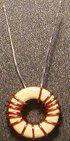
____Remove the PCB from it's plastic bag. Cut a 10" and a 5" wire. Find the yellow toroid.
We will now wind L1, the VCO tank coil. This is the most difficult step.
____Straighten 10" and 5" wires. Remove one inch of insulation off of the 10 and
one end of the 5 inch wires. Tin the stripped wires.
____Hold the toroid with your right hand between your thumb and your index finger, yellow side
toward you. Using your left hand, grab the 10 inch wire 1 inch from the stripped end and
insert the wire through the toroid hole from the top, the yellow side. Wrap the end of the wire
around the toroid to your left. Loop the tinned end through the toroid to your left until less
than one inch of the tinned wire is exposed through the bottom of the toroid.
In your right hand, turn the toroid over so that the non-yellow side is facing you. Using your
left hand, grab the wire and feed it through the top of the toroid, winding to you left until
you have exactly 16 turns of wire through the core of the toroid. Cut the remaining wire to a
length of one inch. Strip the enamel off of the wire all the way to the body of the toroid. Tin
the wire end. Squeeze the wires on the toroid to look like the picture,
 Next, we will add the secondary winding to the Toroid.
Position the windings to look like the picture.
Next, we will add the secondary winding to the Toroid.
Position the windings to look like the picture.
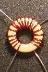 ____Hold the toroid with your right hand between your thumb and your index finger, yellow side
toward you. Using your left hand, grab the 5 inch wire 1 inch from the stripped end and
insert the wire through the toroid hole from the top, the yellow side. Wrap the end of the wire
around the toroid to your left. Loop the tinned end through the toroid to your left until less
than one inch of the tinned wire is exposed through the bottom of the toroid. Place this wire
between the 16 turn winding.
In your right hand, turn the toroid over so that the non-yellow side is facing you. Using your
left hand, grab the wire and feed it through the top of the toroid, winding to you left until
you have exactly 4 turns of wire through the core of the toroid. Cut the remaining wire to a
length of one inch. Strip the enamel off of the wire all the way to the body of the toroid.
Tin the wire end. Addditional help to strip the insulation is here: Striping and Tining
NOTE: All reference/part location descriptions for the PCB are with the writing on top and
the L1 toroid in the lower right corner.
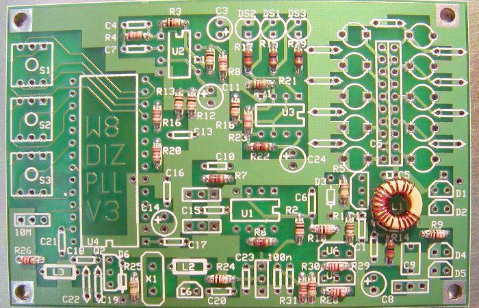
____Mount the completed L1 toroid on the PC board as shown in the picture below and solder
on the bottom of the board. L1's Green Wires insert into the holes on the left side.
Install and solder ALL the resistors.
If you are visually challanged like me, use a magnifying glass to identify the resistors.
Clip the leads close to the board after soldering.
Here is a picture of the PCB with resistors.
____Hold the toroid with your right hand between your thumb and your index finger, yellow side
toward you. Using your left hand, grab the 5 inch wire 1 inch from the stripped end and
insert the wire through the toroid hole from the top, the yellow side. Wrap the end of the wire
around the toroid to your left. Loop the tinned end through the toroid to your left until less
than one inch of the tinned wire is exposed through the bottom of the toroid. Place this wire
between the 16 turn winding.
In your right hand, turn the toroid over so that the non-yellow side is facing you. Using your
left hand, grab the wire and feed it through the top of the toroid, winding to you left until
you have exactly 4 turns of wire through the core of the toroid. Cut the remaining wire to a
length of one inch. Strip the enamel off of the wire all the way to the body of the toroid.
Tin the wire end. Addditional help to strip the insulation is here: Striping and Tining
NOTE: All reference/part location descriptions for the PCB are with the writing on top and
the L1 toroid in the lower right corner.
____Mount the completed L1 toroid on the PC board as shown in the picture below and solder
on the bottom of the board. L1's Green Wires insert into the holes on the left side.
Install and solder ALL the resistors.
If you are visually challanged like me, use a magnifying glass to identify the resistors.
Clip the leads close to the board after soldering.
Here is a picture of the PCB with resistors.
 Suggest you install the resistors in this order:
push all resistors flush against the PCB.
____R5 150K BROWN-GREEN-YELLOW just to the left of the L1 toroid
____R25 150K BROWN-GREEN-YELLOW bottom edge near X1
____R26 220 RED-RED-BROWN bottom left corner
____R29 220 RED-RED-BROWN bottom edge at 7 o'clock from L1
____R28 220 RED-RED-BROWN bottom edge below R29
____R30 1K2 BROWN-RED-RED to the left of R29
____R31 1K5 BROWN-GREEN-RED to the left of R30
____R1 51 GREEN-BROWN-BLACK to the left of L1
____R20 2K7 RED-VIOLET-RED to the right of U4 the PLL chip
____R16 2K7 RED-VIOLET-RED to the right of U4 the PLL chip
____R23 3K9 ORANGE-WHITE_RED to the left of U3 in center of PCB
Nots: R21 used to be a 5K1 resistor. It has been changed to a 3K3.
____R21 3K3 ORANGE-ORANGE-RED above R23
____R8 120 BROWN-RED-BROWN to the left of R21
____R4 27K RED-VIOLET-ORANGE near the top edge above the PLL chip
____R15 1K BROWN-BLACK-RED below DS1 at the top edge of the board
____R17 1K BROWN-BLACK-RED below DS2 at the top edge of the board
____R19 1K BROWN-BLACK-RED below DS3 at the top edge of the board
____R22 1K BROWN-BLACK-RED near the center of the board
____R14 1K BROWN-BLACK-RED below L1
____R6 1K BROWN-BLACK-RED below U1, lower center of board
____R7 1K BROWN-BLACK-RED near the center of the board
____R3 10K BROWN-BLACK-ORANGE near the top of the board
____R11 10K BROWN-BLACK-ORANGE below and right of R3
____R12 10K BROWN-BLACK-ORANGE below R11
____R13 10K BROWN-BLACK-ORANGE to the left of R12
____R18 10K BROWN-BLACK-ORANGE to the right of R12
____R2 10K BROWN-BLACK-ORANGE to the left of L1
____R10 10K BROWN-BLACK-ORANGE to the left of L1
____R9 10K BROWN-BLACK-ORANGE to the right of L1
____R24 10K BROWN-BLACK-ORANGE near bottom center of the board
Installing the Headers.
Only 1 header is required for the PLL, the capacitor bank selector.
Other headers are provided for Power, Tune and 2 headers for the
Freq Counter and Mixer output connections.
Push all headers flush against the PCB and solder.
____Solder a jumper from hole #2 to hole #3 at the 10 meter header
____Cut a 3-pin header and solder for Power; lower right corner
____Cut a 3-pin header and solder for Tune; bottom edge center
____Cut two 3-pin headers and solder for Output; left of U1
____The 10x2 header will be installed in later
Install Power Supply parts and Test.
The PLL uses 2 power supplies, 8 volts and 10 volts. The 10 volt supply
is really closer to 9.7 volts.
____C8 22uF in lower right corner; straighten pins; observe polarity; black band to lower edge.
The next two parts did not get labeled on the PCB correctly. They will both be installed just
to the Right of the Tune Header on the bottom edge of the board. Be aware that all 100n
caps are the same EXCEPT C7 which is a BOX shaped cap that will be installed later.
____C2 100n bottom edge center below label 100n and above label R31
____Cx 100n bottom edge center below label 100n and above label R31
____U5 LM317L between lower edge and L1. Mount U5 1/4 inch above the PCB. Observe case outline.
____U6 LM317L between lower edge and L1. Mount U6 1/4 inch above the PCB. Observe case outline.
Apply power (12-14 volts DC) to the header in the lower right corner. The left most pin
is PLUS(+) and the other two pins are GROUND. Suggest you use the header socket and solder
a WHITE wire to the PLUS(+) and a BLACK wire to one or both GROUND pins.
With power applied, measure the voltage at PIN-3 of the PLL, U4. It should be near 8 volts.
Measure voltage on the (+) side of C24 in the center of the board. It should be near 9.7 volts.
This completes the Power Supply circuit.
Install caps and inductors. Some caps will not be installed until we do the VCO capacitor bank.
push all capacitors flush against the PCB. Mount the inductors 1/16 inch above the PCB.
____C12 100n immediately to the left of R14 and right above C8 and right of label C1.
____C1 100n immediately above the label "C1"
____C23 100n middle of bottom edge
____C20 100n to the left of C23
____C18 100n just below U4, the PLL chip
____C16 100n to the right and center of U4
____C15 100n between the output headers to the left of U1
note: There are 2 types of black toroids: one is shiny, the other dull black.
The dull toroid is an FT37-61 while the shiny is an FT37-43
NOTE: L2 has been changed to a FT37-61 toroid with 20 turns of 26 ga wire. The original inductor
caused too much frequency drift, do to temperature changes. The FT37-61 can be distingished
from the FT37-43 by the color of the toroid. The FT37-43 is shiny, black and smooth, while
the FT37-61 is dull and grayish.
____L2 20 turns on an FT37-61 toroid. Below the output headers. Mount this toroid vertical.
____L3 100uH looks like a resistor in the cap bag BROWN-BLACK-BROWN. Lower left corner.
Substitute is 12 turns on a FT37-43 toroid
____C21 1n marked 102 lower left corner
____C17 1n marked 102 lower right of U4
____C22 56pF lower left corner
____C19 56pF lower left corner next to C22
____C14 22uF lower right of U4; straighten pins; observe the polarity; black band lower edge.
____C13 22n marked 223k; right center of U4
____C11 22uF above C13; straighten pins; observe the polarity; black band toward lower edge.
____C3 22uF middle upper edge; straighten pins; observe the polarity; black band upper edge.
____C24 22uF near center; straighten pins; observe the polarity; black band lower edge.
____C4 10n marked 103; upper left
____C7 100n marked .1J63; below C4; this is the white cap that has a box shape.
____C10 10n marked 103; center of PCB
____C5 15pF just above L1
____C6 10n marked 103; to the left of L1
____C9 1u marked 1uM63, a big blue cap;lower right corner.
____Install 6 YELLOW variable capacitor and 4 ORANGE or WHITE varicaps around the
10x2 header. The BROWN caps are toward the top edge, or the top two rows of varicaps.
The flat side of the caps should always be near the 10x2 header. See the picture below.
____Solder the 10x2 header into the capacitor bank above L1
This completes the installation of the capacitors and inductors. The remaining
capacitors will be used to set up frequency bands.
Install discrete components. (LEDs, Varactors, Diodes, Fets and one Crystal)
____Q1 J310 Fet; just to the left of L1; observe the package outline; flat side right
____Q2 J310 Fet; just below U4; observe the package outline; flat side left
____D7 MV209 Varactor; THIS PART IS INCORRECTLY LABELED D6, below L2 and to the right of X1.
Observe the outline on the board. Mount flush on PCB. Do not overheat when soldering.
____D6 1N4148 just below U4; observe the black band which must be towards the lower edge.
____D3 1N4148 left of L1; observe the black band which must be towards the lower edge.
____D1 MV209 Varactor; right of L1; observe the package outline on the board.
Mount flush on the PCB. Do not overheat when soldering.
____D2 MV209 Varactor; below D1; install just like D1
____D4 MV209 Varactor; below D2; install just like D1
____D5 MV209 Varactor; below D4; install just like D1
note: You may receive a 10.24 or 12.096 XTAL. Either one will work fine in the PLL
____X1 10.24/12.096 Crystal on lower left edge. Push the Xtal into the solder holes. Then
tilt the Xtal about 20 degrees and solder. Straighten the Xtal. This will keep the
Xtal from touching anything under it, preventing shorts. Solder a small bare wire
from the Xtal case to the ground side of R25, (150k left of the Xtal).
____DS1 Green LED top edge. Long lead goes into square solder pad hole
____DS2 Red LED top edge. Long lead goes into square solder pad hole
____DS3 Red LED top edge. Long lead goes into square solder pad hole
Suggest you install the resistors in this order:
push all resistors flush against the PCB.
____R5 150K BROWN-GREEN-YELLOW just to the left of the L1 toroid
____R25 150K BROWN-GREEN-YELLOW bottom edge near X1
____R26 220 RED-RED-BROWN bottom left corner
____R29 220 RED-RED-BROWN bottom edge at 7 o'clock from L1
____R28 220 RED-RED-BROWN bottom edge below R29
____R30 1K2 BROWN-RED-RED to the left of R29
____R31 1K5 BROWN-GREEN-RED to the left of R30
____R1 51 GREEN-BROWN-BLACK to the left of L1
____R20 2K7 RED-VIOLET-RED to the right of U4 the PLL chip
____R16 2K7 RED-VIOLET-RED to the right of U4 the PLL chip
____R23 3K9 ORANGE-WHITE_RED to the left of U3 in center of PCB
Nots: R21 used to be a 5K1 resistor. It has been changed to a 3K3.
____R21 3K3 ORANGE-ORANGE-RED above R23
____R8 120 BROWN-RED-BROWN to the left of R21
____R4 27K RED-VIOLET-ORANGE near the top edge above the PLL chip
____R15 1K BROWN-BLACK-RED below DS1 at the top edge of the board
____R17 1K BROWN-BLACK-RED below DS2 at the top edge of the board
____R19 1K BROWN-BLACK-RED below DS3 at the top edge of the board
____R22 1K BROWN-BLACK-RED near the center of the board
____R14 1K BROWN-BLACK-RED below L1
____R6 1K BROWN-BLACK-RED below U1, lower center of board
____R7 1K BROWN-BLACK-RED near the center of the board
____R3 10K BROWN-BLACK-ORANGE near the top of the board
____R11 10K BROWN-BLACK-ORANGE below and right of R3
____R12 10K BROWN-BLACK-ORANGE below R11
____R13 10K BROWN-BLACK-ORANGE to the left of R12
____R18 10K BROWN-BLACK-ORANGE to the right of R12
____R2 10K BROWN-BLACK-ORANGE to the left of L1
____R10 10K BROWN-BLACK-ORANGE to the left of L1
____R9 10K BROWN-BLACK-ORANGE to the right of L1
____R24 10K BROWN-BLACK-ORANGE near bottom center of the board
Installing the Headers.
Only 1 header is required for the PLL, the capacitor bank selector.
Other headers are provided for Power, Tune and 2 headers for the
Freq Counter and Mixer output connections.
Push all headers flush against the PCB and solder.
____Solder a jumper from hole #2 to hole #3 at the 10 meter header
____Cut a 3-pin header and solder for Power; lower right corner
____Cut a 3-pin header and solder for Tune; bottom edge center
____Cut two 3-pin headers and solder for Output; left of U1
____The 10x2 header will be installed in later
Install Power Supply parts and Test.
The PLL uses 2 power supplies, 8 volts and 10 volts. The 10 volt supply
is really closer to 9.7 volts.
____C8 22uF in lower right corner; straighten pins; observe polarity; black band to lower edge.
The next two parts did not get labeled on the PCB correctly. They will both be installed just
to the Right of the Tune Header on the bottom edge of the board. Be aware that all 100n
caps are the same EXCEPT C7 which is a BOX shaped cap that will be installed later.
____C2 100n bottom edge center below label 100n and above label R31
____Cx 100n bottom edge center below label 100n and above label R31
____U5 LM317L between lower edge and L1. Mount U5 1/4 inch above the PCB. Observe case outline.
____U6 LM317L between lower edge and L1. Mount U6 1/4 inch above the PCB. Observe case outline.
Apply power (12-14 volts DC) to the header in the lower right corner. The left most pin
is PLUS(+) and the other two pins are GROUND. Suggest you use the header socket and solder
a WHITE wire to the PLUS(+) and a BLACK wire to one or both GROUND pins.
With power applied, measure the voltage at PIN-3 of the PLL, U4. It should be near 8 volts.
Measure voltage on the (+) side of C24 in the center of the board. It should be near 9.7 volts.
This completes the Power Supply circuit.
Install caps and inductors. Some caps will not be installed until we do the VCO capacitor bank.
push all capacitors flush against the PCB. Mount the inductors 1/16 inch above the PCB.
____C12 100n immediately to the left of R14 and right above C8 and right of label C1.
____C1 100n immediately above the label "C1"
____C23 100n middle of bottom edge
____C20 100n to the left of C23
____C18 100n just below U4, the PLL chip
____C16 100n to the right and center of U4
____C15 100n between the output headers to the left of U1
note: There are 2 types of black toroids: one is shiny, the other dull black.
The dull toroid is an FT37-61 while the shiny is an FT37-43
NOTE: L2 has been changed to a FT37-61 toroid with 20 turns of 26 ga wire. The original inductor
caused too much frequency drift, do to temperature changes. The FT37-61 can be distingished
from the FT37-43 by the color of the toroid. The FT37-43 is shiny, black and smooth, while
the FT37-61 is dull and grayish.
____L2 20 turns on an FT37-61 toroid. Below the output headers. Mount this toroid vertical.
____L3 100uH looks like a resistor in the cap bag BROWN-BLACK-BROWN. Lower left corner.
Substitute is 12 turns on a FT37-43 toroid
____C21 1n marked 102 lower left corner
____C17 1n marked 102 lower right of U4
____C22 56pF lower left corner
____C19 56pF lower left corner next to C22
____C14 22uF lower right of U4; straighten pins; observe the polarity; black band lower edge.
____C13 22n marked 223k; right center of U4
____C11 22uF above C13; straighten pins; observe the polarity; black band toward lower edge.
____C3 22uF middle upper edge; straighten pins; observe the polarity; black band upper edge.
____C24 22uF near center; straighten pins; observe the polarity; black band lower edge.
____C4 10n marked 103; upper left
____C7 100n marked .1J63; below C4; this is the white cap that has a box shape.
____C10 10n marked 103; center of PCB
____C5 15pF just above L1
____C6 10n marked 103; to the left of L1
____C9 1u marked 1uM63, a big blue cap;lower right corner.
____Install 6 YELLOW variable capacitor and 4 ORANGE or WHITE varicaps around the
10x2 header. The BROWN caps are toward the top edge, or the top two rows of varicaps.
The flat side of the caps should always be near the 10x2 header. See the picture below.
____Solder the 10x2 header into the capacitor bank above L1
This completes the installation of the capacitors and inductors. The remaining
capacitors will be used to set up frequency bands.
Install discrete components. (LEDs, Varactors, Diodes, Fets and one Crystal)
____Q1 J310 Fet; just to the left of L1; observe the package outline; flat side right
____Q2 J310 Fet; just below U4; observe the package outline; flat side left
____D7 MV209 Varactor; THIS PART IS INCORRECTLY LABELED D6, below L2 and to the right of X1.
Observe the outline on the board. Mount flush on PCB. Do not overheat when soldering.
____D6 1N4148 just below U4; observe the black band which must be towards the lower edge.
____D3 1N4148 left of L1; observe the black band which must be towards the lower edge.
____D1 MV209 Varactor; right of L1; observe the package outline on the board.
Mount flush on the PCB. Do not overheat when soldering.
____D2 MV209 Varactor; below D1; install just like D1
____D4 MV209 Varactor; below D2; install just like D1
____D5 MV209 Varactor; below D4; install just like D1
note: You may receive a 10.24 or 12.096 XTAL. Either one will work fine in the PLL
____X1 10.24/12.096 Crystal on lower left edge. Push the Xtal into the solder holes. Then
tilt the Xtal about 20 degrees and solder. Straighten the Xtal. This will keep the
Xtal from touching anything under it, preventing shorts. Solder a small bare wire
from the Xtal case to the ground side of R25, (150k left of the Xtal).
____DS1 Green LED top edge. Long lead goes into square solder pad hole
____DS2 Red LED top edge. Long lead goes into square solder pad hole
____DS3 Red LED top edge. Long lead goes into square solder pad hole
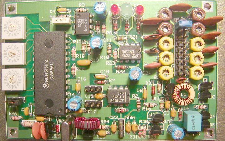 Install all ICs and Switches. You will need to bend the IC pins slightly to easily
insert them into the PCB. The easiest way is to hold an IC perpendicular to a hard
table surface and press down, gently rolling the IC to make a sharp 90 degree bend.
CAUTION: Most of the ICs are CMOS devices and are static senitive.
Be carefull to install the ICs per this picture.
____Install the hex switches S1,S2,S3; mount flush with the PCB.
position the notched corner of the switches with the square soldering hole.
____U3 LM358 near center of PCB; this is the lock detector IC
____U2 LMC662 near top edge; this is the error detect amplifier
____U1 LT1252 near center of PCB; this is the RF output amp
____U4 MC145151P1 the big chip; this is the PLL chip, what makes it all work.
This is a partial finish of the PLL. Before we test the PLL, it is time for
a little THEORY OF OPERATION". Then we will TEST it.
After the test, we will install the capacitor banks which has lots of options.
A VERY BASIC Theory of Operation of the PLL for the multiPIG (PLL-101)
More info can be found here...MC145151P2 PLL Reference (PDF)
Fist, remember that the PLL was designed for the multiPIG, a transceiver with
an IF of 4.914 MHz. Using an IF freq of 4.914 MHz, we want to be able to
transceive on "ALL" frequencies between 1.8 MHz through 27.9 MHz
Doing a little math, we can achieve the 1.8 MHz by mixing a VCO/PLL freq of
6.714 with 1.8 MHz and achive an IF of 4.914. For 10 meters, we mix 29.7 MHz
with an PLL/VCO freq of 24.786 and achive an IF of 4.914 so we have just
calculated that the VCO/PLL must be able to generate from 6.714 through 24.786 MHz.
6.714 - 1.800 = 4.914
29.7 - 24.786 = 4.914
The purpose of the "capacitor bank" in the VCO is to be able to select various amounts
of capacitance to the LC tuned circuit with L1 to oscillate from 6.7 to 24.8 MHz.
We can achieve this with capacitances ranging from about 30 pF to 690 pF.
These values will be selected on the 10x2 header with a shorting jumper. Using the
10x2 header, you can select any frequency band between 1.8 and 29.7 MHz
Each freq band will have a tune range from 5 KHz to 30 KHz, depending upon the band.
Don't let this scare you, as you can select any sub-band using the HEX switches
S1,S2 S3 and the 10 meter jumper switch. Every time you change a sub-band using the
HEX switches, you will increase or decrease the band by 5 KHz. Here is why:
The PLL chip is nothing more than a comparator that generates an ERROR SIGNAL whenever
TWO frequencies are compared and they do no match. The PLL chip compares TWO freqs,
one is from the reference oscillator, generated by the 10.24 MHz XTal and the other
generated by the Voltage Controlled Oscillator.
The reference oscillator is divided down to a lower freq inside the PLL to a preset
amount, in the case of the MC145151P2, it is selectable from 8, 128, 256, 512, 1024,
2048, 2410 and 8192. We will select 2048. Why? If you divide the ref oscillator of
10.24 MHz or 10,240,00 Hz by 2048, you get 5,000 or 5,000 Hz.
The 2nd freq, the one we compare to the reference is the VCO frequency. The input
of the PLL can divide the VCO freq from 3 to 16,383.
The object of the PLL game is to compare TWO frequencies at or near the Ref freq
of 5 KHz and generate an error signal that will be used to correct the VCO freq
to bring it to an exact match with the 5 KHz reference freq.
The HEX switches S1,S2,S3 and the 10 meter select, are used to set the divisor
somewhere in the range of 3 to 16383 so that the VCO divided by the divisor will
approximate 5 KHz. When the VCO freq is lightly higher or lower than the reference
freq of 5 KHz, an error voltage is generated by the PLL chip and filtered into a
clean voltage buy the LMC662 op-amp. It charges a cap, C9 which is fed to the 4
varactor diodes. The error voltage will change the frequency of the VCO to bring
it in line with the ref freq. As you can see, the PLL chip requires 2 inputs and
has one output that goes back to one of the inputs via the VCO varactor diodes,
which goes back into the PLL chip. This is called a closed loop.
Next...
Testing the PLL and ...
How to set the HEX switches to get into a desired frequency band.
TESTING the PLL
Connect a "Tune" pot (labeled R27 on the schematic) to the PLL board.
You can use the Gray 50K pot included with the kit or use your own
tune pot. Most builders will use a 10 turn precision pot with a resistance
of 5K to 100K. Set the tune pot to 50 percent of it's value.
Solder 3 wires (3-12 inches each) to the PCB to the connection point below R6,
bottom center edge of the PCB. The Tune Pot wiper connects to the middle
connection. The other 2 pot connections can be soldered to either of the other
two points.
To test the PLL, you need a receiver capable of receiving
21,060 KHz (15 meters) or a Freq Counter.
Set SW1 to "E" (top hex switch)
Set SW2 to "4" (middle hex switch)
Set SW3 to "5" (bottom hex switch)
NOTE: Review the Cap Bank layout below.
Place the "Capacitor Bank" jumper to the 15 meter position - 3rd from bottom
Adjust the Yellow vari-capacitor (located toward the right of C24) with a
small blade screwdriver or any other tuning tool.
While adjusting the varicap, you should see the LED indicators switching
between Red And Green. If you can adjust the varicap so that the GREEN led
stays on, then you have a good lock condition and the PLL/VCO is working fine.
CONGRATS!!!
If the GREEN LED does not light up, go to the end of this document for help.
The optimum adjustment position for the variable capacitors in the Capacitor
Banks is to adjust the varicaps sot that the HIGH Red LED lights (DS3) and
readjust the varicap until the GREEN Led just comes on. This is the point where
the VCO voltage is at it's hightest.
*** The higher the VCO vlotage, the cleaner the VCO output, especially on the
higher frequencies above 20 MHz. You may want to connect temporary wires to
the varicap voltage and ground and monitor the varactor voltage. A good point
to connect a VOM is across C9, the 1 uF Blue cap in the lower right corner.
The three LED indicators are used as voltage monitors. DS2 (Low) should light
when the Varactor voltage is less than approx 5 volts. DS3 (High) should light
when the varactor voltage is greater than about 9 volts, and DS1 (LOCK) will
light when the varactor voltage is between 5 and 9 volts. Optimum varactor
voltage for the cleanest VCO output is at the high end of LOCK voltage,
7 to 9 volts. Again, this is only critical on VCO outputs greater than 20 MHz.
You can listen to the VCO by monitoring a receiver that can listen to 21,057 KHz.
Connect a sort wire (1 foot) to the VCO output. Connect the wire to the center
point of either of the two connection points to the left of U1.
Tune the "Tune" pot thru its range and listen for a CW note in your receiver.
You can also use a Freq Counter to monitor the Freq at this connection.
HOW TO SET THE HEX SWITCHES TO ANY FREQUENCY using the Calculator that comes with Windows.
Put the Calculator into SCIENTIFIC MODE by clicking on VIEW and selecting SCIENTIFIC.
1. Establish your dersired output frequency. We will use 18,974 KHz because it is the
20 meter QRP freq of 14,060 KHz PLUS the IF of 4,914 MHz
2. Divide the 18,974,000 Hz by the reference frequency of 5,000 Hz and we get 3794.8
Round this off to 3795
3. Enter 3795 into the Calculator and then click on BINARY.
You should get 111011010011
4. Click XOR and enter a ONE (1) thirteen times followed by the "="
It should read 1000100101100
5. Now click HEX and it should read 112C
6. Reverse the digits to read C211
7. To make the VCO lock, you need about 55 pF of total capacitance.
If you look up the freq table you will notice that we
calculated C211 and the table shows A211. Read these digits from left to right as
least significat digit first. The difference is the result of the reference frequency
not being exactly 5000 Hz, but slightly less. If we were to use the exact reference
frequency, then we would end up with A211.
a. Lets use a freq of 7040 exactly since we all can hear it on our favorite receivers.
Also, lets use the measured reference oscillator frequency which is near 4998 Hz
b. Divide the 7,040,000 Hz by the reference frequency of 4998 Hz and we get 1409
c. Enter 1409 into the Calculator and then click on BINARY to get 10110000001
d. Click XOR and enter a ONE (1) thirteen times folloed be the "="
it should read 1101001111110
e. Now click HEX and it should read 1A7E
f. Reverse the digits to read E7A1
g. To make the VCO lock, you need about 600 pF of total capacitance.
BUILDING the CAPACITOR BANK - Establishing the 10 Frequency Bands
The Capacitor Bank circuit was designed to accomodate all 9 HF band plus
the "almost new" 60 meter band. To select a "band", you need to place a
shorting jumper on the 10x2 header. The lowest pair on the hear near L1
is for the 10 meter band. Next up is the 12 meter band, all the way up to
the 80 and 160 meter bands. The complete list from L1 is:
10,12,15,17,20,30,40,60,80 and 160 meters. There is one variable
capacitor associated with each of the 10 HF bands except 10 meters
which has none and 160 metes which has 2.
Calibration of 10 meters:
The YELLOW varicap in the lower left corner of the 2x10 header is placed
into the LC circuit of the VCO when the lowest set of pins on the 2x10
header is shorted with a jumper. See diagram below.
CAPACITOR BANK LAYOUT AND IDENTIFICATION
--------------------------------------------------------
160M FixedCapA upper right corner |
|
[. .]160 |
80M VariCap [. .]80 160M VariCap |
80M FixedCap [. .]60 160M FixedCapB |
40M VariCap [. .]40 60M VariCap |
40M FixedCap [. .]30 60M FixedCap |
20M VariCap [. .]20 30M VariCap |
20M FixedCap [. .]17 30M FixedCap |
15M VariCap [. .]15 17M VariCap |
15M FixedCap [. .]12 17M FixedCap |
10M VariCap [.=.]10 12M VariCap |
__ |
/ \ |
| L1 | |
\ / |
Set the Hex switches to 7ED0. Place jumper over "10"
S1=7, S2=E, S3=D and 0=jumper_is_OFF (toward board edge)
Adjust the "10M VariCap" trimmer until the GREEN LED lights.
Calibration of 12 meters:
Set the Hex switches to 0601. Place jumper ofver "12"
S1=0, S2=6, S3=0 and 1=jumper_is_ON (toward U4)
Adjust the "12M VariCap" trimmer until the GREEN LED lights.
Do the same proceedure for the other bands.
NOTE: Bands higher that 12 meters need additional capacitance
to resonate on the desired bands. Solder the required capacitors
associated with each band into it's correct location. Example:
note: Use the above digram as a reference. There are no labels
for the band caps. The reason for this is that you can customize
the capacitor bank for ANY frequencies between 1.8 and 30 MHz
The PLL is NOT just a Ham Band Frequency Generator.
Solder a 56pF cap into the location labeled "15M FixedCap"
Solder a 100pF cap into the location labeled "17M FixedCap"
Solder a 33pF cap into the location labeled "20M FixedCap"
Solder a 56pF cap into the location labeled "30M FixedCap"
Solder a 130pF cap into the location labeled "40M FixedCap"
Solder a 220pF cap into the location labeled "60M FixedCap"
Solder a 330pF cap into the location labeled "80M FixedCap"
Solder a 330pF cap into the locations labeled "160M FixedCapA"
Solder a 220pF cap into the locations labeled "160M FixedCapB"
Here are the suggested Ham Band settings for the PLL switch
and the 10 meter jumper.
As an example for 40 meters:
Hex Switch S1 is set to "7"
Hex Switch S2 is set to "A"
Hex Switch S1 is set to "6
10 meter jumper toward U4"
10 7ED0 Jumper toward left edge of board
12 0601 Jumper toward U4
15 2631 Jumper toward U4
17 4B51 Jumper toward U4
20 A211 Jumper toward U4
30 1441 Jumper toward U4
40 7A61 Jumper toward U4
60 3081 Jumper toward U4
80 F591 Jumper toward U4
160 DBA1 Jumper toward U4
The above PLL HEX switch settings also require that you place a jumper
on the appropriate Capacitor Bank selection.
EXTRA HOLES IN THE PLL PCB (optional VCO tune cap)
In the lower right edge of the PLL board, between a yellow varicap
and L1 are 2 solder holes. One is ground, the other is an optional
connection to an external variable capacitor. You can connect a
365 pF broadcast cap here to allow you to tune the VCO over a very
wide frequency range, depending upon the PLL Hex Switch settings.
Just be aware that this capacitor needs a good ground connection
and also must be mounted in such a way as to avoid microphonics.
Any vibration on the broadcast cap with show up in the output
of the PLL.
A NOTE ABOUT THE LEDs/LM358 LOCK INDICATOR CIRCUIT. It's purpose is
to let the operator know if the VCO varicaps are at a low voltage,
a nominal LOCK voltage or a high voltage. When the varactor voltages
are too high or too low, the PLL may be out of lock. One thing about
varactors, their Q goes up when the reverse voltage is increased and
we want as high a Q as possible for the best and cleanest VCO oscillations.
The LM358 is configured as TWO voltage comparators. One switches at
5.1 volts and the other at 9 volts. Look at resistors R21, 22 and 23.
They make up the reference voltage divisors. PIN3 is set at 5.1 volts
When PIN2 is LOWER than 5.1 volts, the output on PIN1 goes HIGH turning
on LED DS2. The output of PIN7 is also HIGH which prevent the other 2
LEDs from turning on. When the input voltage on PIN2 and PIN6 goes
between 5.1 and 9 volts, PIN1 goes LOW but PIN7 is still HIGH which
turns on ONLY LED DS1, the LOCK indicator. Onces the voltage at the
inputs exceed 9 volts, both op-amp outputs go LOW which will turn
on LED DS3. Pretty simple eh?
HELP!!! What to do if you can't get the PLL's GREEN LED to turn on.
Email me ... w8diz at fpqrp.com
Install all ICs and Switches. You will need to bend the IC pins slightly to easily
insert them into the PCB. The easiest way is to hold an IC perpendicular to a hard
table surface and press down, gently rolling the IC to make a sharp 90 degree bend.
CAUTION: Most of the ICs are CMOS devices and are static senitive.
Be carefull to install the ICs per this picture.
____Install the hex switches S1,S2,S3; mount flush with the PCB.
position the notched corner of the switches with the square soldering hole.
____U3 LM358 near center of PCB; this is the lock detector IC
____U2 LMC662 near top edge; this is the error detect amplifier
____U1 LT1252 near center of PCB; this is the RF output amp
____U4 MC145151P1 the big chip; this is the PLL chip, what makes it all work.
This is a partial finish of the PLL. Before we test the PLL, it is time for
a little THEORY OF OPERATION". Then we will TEST it.
After the test, we will install the capacitor banks which has lots of options.
A VERY BASIC Theory of Operation of the PLL for the multiPIG (PLL-101)
More info can be found here...MC145151P2 PLL Reference (PDF)
Fist, remember that the PLL was designed for the multiPIG, a transceiver with
an IF of 4.914 MHz. Using an IF freq of 4.914 MHz, we want to be able to
transceive on "ALL" frequencies between 1.8 MHz through 27.9 MHz
Doing a little math, we can achieve the 1.8 MHz by mixing a VCO/PLL freq of
6.714 with 1.8 MHz and achive an IF of 4.914. For 10 meters, we mix 29.7 MHz
with an PLL/VCO freq of 24.786 and achive an IF of 4.914 so we have just
calculated that the VCO/PLL must be able to generate from 6.714 through 24.786 MHz.
6.714 - 1.800 = 4.914
29.7 - 24.786 = 4.914
The purpose of the "capacitor bank" in the VCO is to be able to select various amounts
of capacitance to the LC tuned circuit with L1 to oscillate from 6.7 to 24.8 MHz.
We can achieve this with capacitances ranging from about 30 pF to 690 pF.
These values will be selected on the 10x2 header with a shorting jumper. Using the
10x2 header, you can select any frequency band between 1.8 and 29.7 MHz
Each freq band will have a tune range from 5 KHz to 30 KHz, depending upon the band.
Don't let this scare you, as you can select any sub-band using the HEX switches
S1,S2 S3 and the 10 meter jumper switch. Every time you change a sub-band using the
HEX switches, you will increase or decrease the band by 5 KHz. Here is why:
The PLL chip is nothing more than a comparator that generates an ERROR SIGNAL whenever
TWO frequencies are compared and they do no match. The PLL chip compares TWO freqs,
one is from the reference oscillator, generated by the 10.24 MHz XTal and the other
generated by the Voltage Controlled Oscillator.
The reference oscillator is divided down to a lower freq inside the PLL to a preset
amount, in the case of the MC145151P2, it is selectable from 8, 128, 256, 512, 1024,
2048, 2410 and 8192. We will select 2048. Why? If you divide the ref oscillator of
10.24 MHz or 10,240,00 Hz by 2048, you get 5,000 or 5,000 Hz.
The 2nd freq, the one we compare to the reference is the VCO frequency. The input
of the PLL can divide the VCO freq from 3 to 16,383.
The object of the PLL game is to compare TWO frequencies at or near the Ref freq
of 5 KHz and generate an error signal that will be used to correct the VCO freq
to bring it to an exact match with the 5 KHz reference freq.
The HEX switches S1,S2,S3 and the 10 meter select, are used to set the divisor
somewhere in the range of 3 to 16383 so that the VCO divided by the divisor will
approximate 5 KHz. When the VCO freq is lightly higher or lower than the reference
freq of 5 KHz, an error voltage is generated by the PLL chip and filtered into a
clean voltage buy the LMC662 op-amp. It charges a cap, C9 which is fed to the 4
varactor diodes. The error voltage will change the frequency of the VCO to bring
it in line with the ref freq. As you can see, the PLL chip requires 2 inputs and
has one output that goes back to one of the inputs via the VCO varactor diodes,
which goes back into the PLL chip. This is called a closed loop.
Next...
Testing the PLL and ...
How to set the HEX switches to get into a desired frequency band.
TESTING the PLL
Connect a "Tune" pot (labeled R27 on the schematic) to the PLL board.
You can use the Gray 50K pot included with the kit or use your own
tune pot. Most builders will use a 10 turn precision pot with a resistance
of 5K to 100K. Set the tune pot to 50 percent of it's value.
Solder 3 wires (3-12 inches each) to the PCB to the connection point below R6,
bottom center edge of the PCB. The Tune Pot wiper connects to the middle
connection. The other 2 pot connections can be soldered to either of the other
two points.
To test the PLL, you need a receiver capable of receiving
21,060 KHz (15 meters) or a Freq Counter.
Set SW1 to "E" (top hex switch)
Set SW2 to "4" (middle hex switch)
Set SW3 to "5" (bottom hex switch)
NOTE: Review the Cap Bank layout below.
Place the "Capacitor Bank" jumper to the 15 meter position - 3rd from bottom
Adjust the Yellow vari-capacitor (located toward the right of C24) with a
small blade screwdriver or any other tuning tool.
While adjusting the varicap, you should see the LED indicators switching
between Red And Green. If you can adjust the varicap so that the GREEN led
stays on, then you have a good lock condition and the PLL/VCO is working fine.
CONGRATS!!!
If the GREEN LED does not light up, go to the end of this document for help.
The optimum adjustment position for the variable capacitors in the Capacitor
Banks is to adjust the varicaps sot that the HIGH Red LED lights (DS3) and
readjust the varicap until the GREEN Led just comes on. This is the point where
the VCO voltage is at it's hightest.
*** The higher the VCO vlotage, the cleaner the VCO output, especially on the
higher frequencies above 20 MHz. You may want to connect temporary wires to
the varicap voltage and ground and monitor the varactor voltage. A good point
to connect a VOM is across C9, the 1 uF Blue cap in the lower right corner.
The three LED indicators are used as voltage monitors. DS2 (Low) should light
when the Varactor voltage is less than approx 5 volts. DS3 (High) should light
when the varactor voltage is greater than about 9 volts, and DS1 (LOCK) will
light when the varactor voltage is between 5 and 9 volts. Optimum varactor
voltage for the cleanest VCO output is at the high end of LOCK voltage,
7 to 9 volts. Again, this is only critical on VCO outputs greater than 20 MHz.
You can listen to the VCO by monitoring a receiver that can listen to 21,057 KHz.
Connect a sort wire (1 foot) to the VCO output. Connect the wire to the center
point of either of the two connection points to the left of U1.
Tune the "Tune" pot thru its range and listen for a CW note in your receiver.
You can also use a Freq Counter to monitor the Freq at this connection.
HOW TO SET THE HEX SWITCHES TO ANY FREQUENCY using the Calculator that comes with Windows.
Put the Calculator into SCIENTIFIC MODE by clicking on VIEW and selecting SCIENTIFIC.
1. Establish your dersired output frequency. We will use 18,974 KHz because it is the
20 meter QRP freq of 14,060 KHz PLUS the IF of 4,914 MHz
2. Divide the 18,974,000 Hz by the reference frequency of 5,000 Hz and we get 3794.8
Round this off to 3795
3. Enter 3795 into the Calculator and then click on BINARY.
You should get 111011010011
4. Click XOR and enter a ONE (1) thirteen times followed by the "="
It should read 1000100101100
5. Now click HEX and it should read 112C
6. Reverse the digits to read C211
7. To make the VCO lock, you need about 55 pF of total capacitance.
If you look up the freq table you will notice that we
calculated C211 and the table shows A211. Read these digits from left to right as
least significat digit first. The difference is the result of the reference frequency
not being exactly 5000 Hz, but slightly less. If we were to use the exact reference
frequency, then we would end up with A211.
a. Lets use a freq of 7040 exactly since we all can hear it on our favorite receivers.
Also, lets use the measured reference oscillator frequency which is near 4998 Hz
b. Divide the 7,040,000 Hz by the reference frequency of 4998 Hz and we get 1409
c. Enter 1409 into the Calculator and then click on BINARY to get 10110000001
d. Click XOR and enter a ONE (1) thirteen times folloed be the "="
it should read 1101001111110
e. Now click HEX and it should read 1A7E
f. Reverse the digits to read E7A1
g. To make the VCO lock, you need about 600 pF of total capacitance.
BUILDING the CAPACITOR BANK - Establishing the 10 Frequency Bands
The Capacitor Bank circuit was designed to accomodate all 9 HF band plus
the "almost new" 60 meter band. To select a "band", you need to place a
shorting jumper on the 10x2 header. The lowest pair on the hear near L1
is for the 10 meter band. Next up is the 12 meter band, all the way up to
the 80 and 160 meter bands. The complete list from L1 is:
10,12,15,17,20,30,40,60,80 and 160 meters. There is one variable
capacitor associated with each of the 10 HF bands except 10 meters
which has none and 160 metes which has 2.
Calibration of 10 meters:
The YELLOW varicap in the lower left corner of the 2x10 header is placed
into the LC circuit of the VCO when the lowest set of pins on the 2x10
header is shorted with a jumper. See diagram below.
CAPACITOR BANK LAYOUT AND IDENTIFICATION
--------------------------------------------------------
160M FixedCapA upper right corner |
|
[. .]160 |
80M VariCap [. .]80 160M VariCap |
80M FixedCap [. .]60 160M FixedCapB |
40M VariCap [. .]40 60M VariCap |
40M FixedCap [. .]30 60M FixedCap |
20M VariCap [. .]20 30M VariCap |
20M FixedCap [. .]17 30M FixedCap |
15M VariCap [. .]15 17M VariCap |
15M FixedCap [. .]12 17M FixedCap |
10M VariCap [.=.]10 12M VariCap |
__ |
/ \ |
| L1 | |
\ / |
Set the Hex switches to 7ED0. Place jumper over "10"
S1=7, S2=E, S3=D and 0=jumper_is_OFF (toward board edge)
Adjust the "10M VariCap" trimmer until the GREEN LED lights.
Calibration of 12 meters:
Set the Hex switches to 0601. Place jumper ofver "12"
S1=0, S2=6, S3=0 and 1=jumper_is_ON (toward U4)
Adjust the "12M VariCap" trimmer until the GREEN LED lights.
Do the same proceedure for the other bands.
NOTE: Bands higher that 12 meters need additional capacitance
to resonate on the desired bands. Solder the required capacitors
associated with each band into it's correct location. Example:
note: Use the above digram as a reference. There are no labels
for the band caps. The reason for this is that you can customize
the capacitor bank for ANY frequencies between 1.8 and 30 MHz
The PLL is NOT just a Ham Band Frequency Generator.
Solder a 56pF cap into the location labeled "15M FixedCap"
Solder a 100pF cap into the location labeled "17M FixedCap"
Solder a 33pF cap into the location labeled "20M FixedCap"
Solder a 56pF cap into the location labeled "30M FixedCap"
Solder a 130pF cap into the location labeled "40M FixedCap"
Solder a 220pF cap into the location labeled "60M FixedCap"
Solder a 330pF cap into the location labeled "80M FixedCap"
Solder a 330pF cap into the locations labeled "160M FixedCapA"
Solder a 220pF cap into the locations labeled "160M FixedCapB"
Here are the suggested Ham Band settings for the PLL switch
and the 10 meter jumper.
As an example for 40 meters:
Hex Switch S1 is set to "7"
Hex Switch S2 is set to "A"
Hex Switch S1 is set to "6
10 meter jumper toward U4"
10 7ED0 Jumper toward left edge of board
12 0601 Jumper toward U4
15 2631 Jumper toward U4
17 4B51 Jumper toward U4
20 A211 Jumper toward U4
30 1441 Jumper toward U4
40 7A61 Jumper toward U4
60 3081 Jumper toward U4
80 F591 Jumper toward U4
160 DBA1 Jumper toward U4
The above PLL HEX switch settings also require that you place a jumper
on the appropriate Capacitor Bank selection.
EXTRA HOLES IN THE PLL PCB (optional VCO tune cap)
In the lower right edge of the PLL board, between a yellow varicap
and L1 are 2 solder holes. One is ground, the other is an optional
connection to an external variable capacitor. You can connect a
365 pF broadcast cap here to allow you to tune the VCO over a very
wide frequency range, depending upon the PLL Hex Switch settings.
Just be aware that this capacitor needs a good ground connection
and also must be mounted in such a way as to avoid microphonics.
Any vibration on the broadcast cap with show up in the output
of the PLL.
A NOTE ABOUT THE LEDs/LM358 LOCK INDICATOR CIRCUIT. It's purpose is
to let the operator know if the VCO varicaps are at a low voltage,
a nominal LOCK voltage or a high voltage. When the varactor voltages
are too high or too low, the PLL may be out of lock. One thing about
varactors, their Q goes up when the reverse voltage is increased and
we want as high a Q as possible for the best and cleanest VCO oscillations.
The LM358 is configured as TWO voltage comparators. One switches at
5.1 volts and the other at 9 volts. Look at resistors R21, 22 and 23.
They make up the reference voltage divisors. PIN3 is set at 5.1 volts
When PIN2 is LOWER than 5.1 volts, the output on PIN1 goes HIGH turning
on LED DS2. The output of PIN7 is also HIGH which prevent the other 2
LEDs from turning on. When the input voltage on PIN2 and PIN6 goes
between 5.1 and 9 volts, PIN1 goes LOW but PIN7 is still HIGH which
turns on ONLY LED DS1, the LOCK indicator. Onces the voltage at the
inputs exceed 9 volts, both op-amp outputs go LOW which will turn
on LED DS3. Pretty simple eh?
HELP!!! What to do if you can't get the PLL's GREEN LED to turn on.
Email me ... w8diz at fpqrp.com