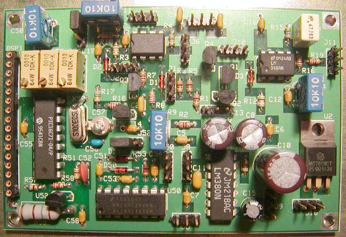
INSTRUCTIONS FOR BUILDING THE FCC, A component of the multiPIG+
(updated 12-09-2003)

The FCC kit includes 3 plastic envelopes, an LCD display and a set
of drawings, 6 feet wire and references documents.
  1. PCB
  2. Semiconductors and Connectors
  3. Resistors and ICs
  4. LCD display,

We will build the FCC in this order:
  1. Install the Crystal
  2. Install all resistors
  3. Install all capacitors
  4. Install all transistors and regulators
  5. Install diodes
  6. install all headers
  7. Install LCD socket
  8. Test voltage regulators
  9. Install all ICs and Pots
 10. Calibrate Freq Counter
 11. Calibrate AGC
 12. Discuss the K10 keyer chip operation
 13. Test T/R switching

You may want to consider the following items NOT included in the kit:
1. Miniature coax for interconnections ( I will have some available soon)
2. External SPDT switch for setting the IF freq offset for the FreqCounter.
   A jumper will be supplied
3. On/Off switch with volume control (10K is good)
4. External CW Speed pot (10K) to replace R11 on the PCB.
5. Push Button switch to activate the speed pot.
6. Push putton to place the Keyer chip into the "Command" mode.


Ready...set...begin!

____Remove the PCB from it's plastic bag. Do a general inspection of the PCB

____Install the 10 MHz XTAL at X50. Insert the XTAL from the top of the PCB and
    tilt it to one side about 20 or 25 degrees and solder on bottom of board.
    After soldering, remove excess leads and straighten the XTAL into a vertical position
    This process should leave a small space under the XTAL to prevent the metal case shorting

____Install a small one inch wire into the hole just to the right of the text "X50".
    Solder this wire between the hole and the top of the Crystal. See picture on Web page.

Install and solder ALL the resistors.
If you are visually challanged like me, use a magnifying glass to identify the resistors.
Clip the leads close to the board after soldering.

Suggest you install the resistors in this order:
push all resistors flush against the PCB and solder, then clip leads flush.

____R51 430 YELLOW-ORANGE-BROWN just below the crystal
____R52 10K BROWN-BLACK_ORANGE near upper left corner
____R53  1K BROWN-BLACK-RED above pin 11 of U50
____R57 680 BLUE-GRAY-BROWN near lower left corner
____R58 220 RED-RED-BROWN to the right of R57

install either a 180 or 200 ohm 2 watt resistor at R59
There is a slight bend on the lead that installs near the screw hole
See the picture of the lead-bend on the "FCC-TOP.gif" picture.
____R59 180 2 watts BROWN-GRAY-BROWN lower left corner
____R59 200 2 watts RED-BLACK-BROWN lower left corner

next 5 resistors may have a 3K3 value
____R1   3K ORANGE-BLACK-RED near center of board
____R2   3K ORANGE-BLACK-RED below R1
____R5   3K ORANGE-BLACK-RED above R1
____R6   3K ORANGE-BLACK-RED left of R5
____R7   3K ORANGE-BLACK-RED below U1

____R3  15K BROWN-GREEN-ORANGE to the left of U1
____R4  5K1 GREEN-BROWN-RED to the right of U1
____R8  27K RED-VIOLET-ORANGE below Pin3 of U1
____R10 10K BROWN-BLACK-ORANGE to the left of U1 below speed pot R11
____R16 10K BROWN-BLACK-ORANGE immediately to the right of U3
____R12 51K GREEN-BROWN-ORANGE below Pin1 of U3

____R13 4R7 YELLOW-VIOLET-GOLD to the right of U4
____R15 4M7 YELLOW-VIOLET-GREEN above Pin5 of U3
____R17 750 VIOLET-GREEN-BROWN top right next to the crystal
____R18 220 RED-RED-BROWN top right next to the crystal
____R19 5K1 GREEN-BROWN-RED right of U3

Install diodes

____D50 1N4148 - above U50
____D51 1N4148 - above U50
____D1  1N4148 - below Pin4 of U1
____D2  1N4148 - between Xtal and U1

NOTE: The next diode is used to detect the audio voltage for the AGC amp.
      The orignial MP used a 1N4148 and it worked well but I include an
		optional 1N5711 schottky diode, which I use in my MP+. The 1N5711
		will give you a lower AGC threshhold. This means that the 1N5711
		will activate the AGC system before the 1N4148. My suggestion it
		that you install the 1N5711.
____D3 1N4148 or 1N5711 - to the left of U3


Installation of the Capacitors.

NOTE: C57 can be either a ceramic or plastic coated trim cap
____C57 If ceramic Trim Cap - install the trim cap to the right
    of the xtal with the small tab side toward the crystal.
    If plastic trim cap - install with flat side toward Crystal.
____C56 43p or 47p - lower right of the xtal NOTE: may have shipped the wrong
    version cap with a lead spacing of 0.2" not 0.1" as required. Sorry!
    Do the best you can to fit the 43pF cap into slot C56. Future kits
    will have the correct 0.1" spacing cap.
____C52 220p - orange disc cap below the crystal.
____C50 100n - upper left cornet
____C51 100n - above Pin16 of U50
____C53 100n - above U50
____C54 100n - above Pin10 of U50
____C55 100n - left of U51
____C58 100n - left bottom of U50

note: C2,3 and 4 can be either 6n8 (blue) or 10n (yellow) caps
____C2   6n8 - between center of PCB and the crystal (10n opt)
____C3   6n8 - top edge middle of the board (10n opt)
____C4   6n8 - top edge middle of the board (10n opt)
____C11  47n - left of U4 (marked 473)
____C1  100n - immediately to the left of U1
____C5  100n - near middle of the board
____C6  100n - middle of board toward the right
____C7  100n - middle of board toward the lower edge
____C12 100n - below Pin4 of U3
____C14 100n - right of XTal toward middle of board
____C16 100n - top edge of board toward the right
____C17 100n - between Xtal and the top board edge

____C13 470n - upper right corner (marked .47)
____C15 100uF - to the right of Pin9 of U4
____C8  220uF - above U4
____C9  220uF - above U4
____C10 680uF or 470uF - right of U4

Install all transistors and regulators

____U52 LM317LZ - lower left corner of board. Observe outline.
____U5  LM317LZ - towards the middle of board. Observe outline.
____Q3  2N3904 - upper right of Xtal. Observe outline
____Q1  2N3906 - between U4 and the top board edge
____Q2  2N3906 - between U4 and the top board edge
____Q4  2N3906 - between U4 and the top board edge

Installing ALL the 3-pin Headers with the short end inserted into the top
of the PCB and solder on the bottom of the board. Don't burn your fingers.
There are 15 of them.

____J50 lower center of PCB above pin-9 of U50
____J51 upper edge toward left
____J52 to the right of the Crystal

____J1 slightly above the center of PCB
____J2 below pin-1 of U1
____J3 - NOT INSTALLED - has been removed from circuit
____J4 near center upper edge
____J5 middle of the bottom edge of PCB
____J6 to the right of U1, upper center of PCB
____J7 near center upper edge
____J8 left of U4, lower center of PCB
____J9 near lower right corner
____J10 lower right corner
____J11 upper right corner
____J12 near pin-8 of U3, upper middle right of PCB
____J13 center of PCB slightly right

There are many ways to wire up the LCD display...here is one...
NOTE: To correctly view the LCD display, the LCD wire connections are on top.
Install the LCD machine pin sockets - there is a 16 pin machine SIP socket
or a 7 and 9 pin SIP machine sockets. Solder on top of the PCB.
Decide how far you want the LCD display to be away from the FCC PCB.
I would recommend 4 inches or less. Cut 16 equal size wires from the 6 foot
coil of wire. Strip 1/8th inch of insulation from each end.
Solder the 16 wires into the 16 holes of the LCD display. Recommend that you
insert the wires from the top and solder on the bottom. Once soldered,
plug each wire into the machine socket on the PCB.

The IMPORTANT thing to do is wire up the display to the 16 pin socket starting at
pin-1 on the display to pin-1 on the 16 pin socket (top) and work down until all 16
connections are made to the display.  The last 2 connections on the 16 pin socket
are for the backlight display on the LCD.


Install U2, the 7808 voltage regulator. Bend the smaller part of the IC's legs
down at a right angle. Insert into the PCB so the IC's hole aligns with the PCB.
Make sure the flat side of the regulator is flush against the PCB.
Solder and trim.


Test Power Supply - voltage regulators
Apply 12 volts to J10 (lower right corner)
You should measure 5 volts on Pin16 of U50
and 5.5 volts on the center pin of U5
and 8 volts on the right pin of U2
If any of these voltages are different, stop
and recheck you work.
Remove power from the FCC.

Install all ICs

Bend the leads on all the IC's perpendicular to the body of the IC.
This is easiest done by placing one side of an IC flat on a table top
and pressing down to remove the slight curve from the body of the IC.
Install the following devices observing Pin-1 polarity

____U50 74HC4046 - 16 pin dip
____U51 PIC16C71 - 18 pin dip

____U1 K10 8 pin dip - this part # starts with a 12
____U3 LM358 8 pin dip
____U4 LM380 14 pin dip

Install all Potentiometers

____R9  10K 1 turn (Blue pot) center of PCB
____R11 10K 1 turn (Blue pot) top edge near center
____R14 10K 1 turn (Blue pot) near right edge
____R50 10K 1 turn (Blue pot) upper left corner


Mount the next 3 pots with the adjustment screws towards U51
note: These 3 pots can be any value form 10K to 100K
____R54 10k 10 turn (Yellow or Blue pot) above U51
____R55 10k 10 turn (Yellow or Blue pot) above U51
____R56 10k 10 turn (Yellow or Blue pot) above U51

Calibrate Freq Counter:
Connect a jumper on J52 (right of Xtal) on the left 2 pins.
Connect a jumper on J51 (upper left edge) on the upper two pins.
Connect the LCD to the main PCB.
Power up the FCC with 12V on J10 (lower right corner)
Note: Center pin on J10 is +12; the other pins are ground or (-)

The total current consumed by the FCC should be about than 50 MA with
the LCD backlight OFF and about 90 MA with the backlight ON.
Adjust the contrast of the LDC display via R50 (upper left corner).
Adjust R54,R55 and R56 all the way CW or CCW to get a ZERO reading on the LCD.
Move the jumper on J51 (upper left edge) to the lower two pins.
Connect a known frequency source to J50 (above pin-9 of U50).
All you need to do is connect the center pin of J50 to a stable RF source.
A 15 meter signal is ideal.
With the KNOWN RF source applied, adjust C57 (right of the Xtal) until the
displayed Frequency matches the known source.  Next we will adjust the IF
offset pots. Remove the RF calibration source from J50 above pin-9 of U50).
Short the input at J50 to ground.
Move the jumper on J51 (upper left edge) to the lower two pins.
From left to right, the IF offset pots are:
R54 - course IF offest
R55 - fine IF offset
R56 - medium IF offset
Note: The display will show frequecies in 10 Hz increments.

Adjust R54 for maximum count display, but LESS THAN 4,913,70
Adjust R56 for maximum count display, but LESS THAN 4,913,70
NOTE#1: If you have trouble setting R56, see note#1 at bottom.
Adjust R55 to exactly 4,913,70
This completes the IF offset adjustment. When you build the receiver kit, we will
calibrate the IF offset EXACTLY to the center frequency of the crystal filter.

Note: J51 (upper left corner) is used to enable/disable the IF offset for the freq
counter. Jumper the upper two pins to enable the IF offset, lower 2 pins to disable.
J52 (right of Xtal) is used to either add or subtract the IF offset from the input
frequency. Jumper the left 2 pins for (+) and right 2 pins for (-).
Leave the jumpers connected to J51 and J52.

Calibrate AGC
Connect a voltmeter to the center pin of J11 (upper right) and ground (mounting holes)
Adjust R14 (next to J11) for a 5.0 volt reading on the voltmeter.

Test K10 keyer and Audio Amp and adjust sidetone.
Remove the 12V power from the FCC (J10 lower right corner).
Install a volume control pot on J8 (lower center). Any pot from 10K to 100K
Connect the center pot wiper to Pin-2 of J8. Connect the other two
pot connections to Pins 1 and 3. If you get the volume pot backwards,
you can correct it later. Connect a speaker to J9 (lower right).
Reconnect the 12V power (J10 lower right corner).
Touch the center pin on the volume control. You should hear a 60 Hz hum.
You may have to set the volume control to one end or the other.

NOTE: The volume control on J8 (lower center)will have no effect on the
sidetone volume.
While shorting the left two pins of J4 (upper edge), the Paddle connector,
adjust R9 (center of PCB) for a comfortable listening level of the sidetone.
Remove the short on J4 (upper edge).

Additional K10 keyer chip Tests:
If you have a set of paddles available, connect to J4 (upper edge).
the "dit" connects to the right pin of J4 and the "dah" to the left pin.
The center pin is "common" or ground.
Test your Paddles. You should hear dits and dahs from the speaker.

Momentary short and release the upper two pins of J6 (upper center).
You should hear (in CW) the letters "MT". This is short for "Empty",
refering to the message buffer in the K10 chip.
Short and HOLD the upper two pins of J6 (upper center) until you hear
the letter "R" in CW, then release. This indicated that the K10 chip is
ready to receive a command via the paddles.
Short and HOLD the upper two pins of J6 (upper center) until you hear
a series of "dits". This indicates the K10 chip has been reset to default mode.

For more info on the K10 chip click the link:
          K10 Manual in PDF format

Test T/R switching: (with 12V power applied to J10 (lower right corner).
Measure the voltage on the center pin of J13 (center of PCB) to ground.
It should be about 7.8 Volts.
Measure the voltage on the center pin of J12 (upper center) to ground.
It should be less than 0.5 volts.
Place a short or jumper over left 2 pins of J2 (upper left center).
Measure the voltage on the center pin of J13 (center right) to ground.
It should be less than 0.5 Volts.
Measure the voltage on the center pin of J12 (upper center) to ground.
It should be about 7.8 Volts.
remove the short from J2 (upper left center).
Note: J2 can be used as a "XMTR TUNE" connection via a switch (your stock).

THAT COMPLETES THE TESTING OF THE FCC


HELP!!! What to do if you can't get the FCC to work?
Email me ... w8diz at fpqrp.com

NOTE#1:
Solder a 150 ohm +/- 50 ohms resistor between the wiper of R56
and the +5 side of R56. Then readjust the medium offset pot.
*** DO THIS ONLY WITH THE WIPER NEAR 5 VOLT POTENTIAL. ***
Problem is that the CPU has a hard time reading voltages that are
close the the Vcc (+5V) limit. The addition of the resistor will
greatly enhance your adjusting resolution, but only at the +5 end.
Ready...set...begin!
____Remove the PCB from it's plastic bag. Do a general inspection of the PCB
____Install the 10 MHz XTAL at X50. Insert the XTAL from the top of the PCB and
tilt it to one side about 20 or 25 degrees and solder on bottom of board.
After soldering, remove excess leads and straighten the XTAL into a vertical position
This process should leave a small space under the XTAL to prevent the metal case shorting
____Install a small one inch wire into the hole just to the right of the text "X50".
Solder this wire between the hole and the top of the Crystal. See picture on Web page.
Install and solder ALL the resistors.
If you are visually challanged like me, use a magnifying glass to identify the resistors.
Clip the leads close to the board after soldering.
Suggest you install the resistors in this order:
push all resistors flush against the PCB and solder, then clip leads flush.
____R51 430 YELLOW-ORANGE-BROWN just below the crystal
____R52 10K BROWN-BLACK_ORANGE near upper left corner
____R53 1K BROWN-BLACK-RED above pin 11 of U50
____R57 680 BLUE-GRAY-BROWN near lower left corner
____R58 220 RED-RED-BROWN to the right of R57
install either a 180 or 200 ohm 2 watt resistor at R59
There is a slight bend on the lead that installs near the screw hole
See the picture of the lead-bend on the "FCC-TOP.gif" picture.
____R59 180 2 watts BROWN-GRAY-BROWN lower left corner
____R59 200 2 watts RED-BLACK-BROWN lower left corner
next 5 resistors may have a 3K3 value
____R1 3K ORANGE-BLACK-RED near center of board
____R2 3K ORANGE-BLACK-RED below R1
____R5 3K ORANGE-BLACK-RED above R1
____R6 3K ORANGE-BLACK-RED left of R5
____R7 3K ORANGE-BLACK-RED below U1
____R3 15K BROWN-GREEN-ORANGE to the left of U1
____R4 5K1 GREEN-BROWN-RED to the right of U1
____R8 27K RED-VIOLET-ORANGE below Pin3 of U1
____R10 10K BROWN-BLACK-ORANGE to the left of U1 below speed pot R11
____R16 10K BROWN-BLACK-ORANGE immediately to the right of U3
____R12 51K GREEN-BROWN-ORANGE below Pin1 of U3
____R13 4R7 YELLOW-VIOLET-GOLD to the right of U4
____R15 4M7 YELLOW-VIOLET-GREEN above Pin5 of U3
____R17 750 VIOLET-GREEN-BROWN top right next to the crystal
____R18 220 RED-RED-BROWN top right next to the crystal
____R19 5K1 GREEN-BROWN-RED right of U3
Install diodes
____D50 1N4148 - above U50
____D51 1N4148 - above U50
____D1 1N4148 - below Pin4 of U1
____D2 1N4148 - between Xtal and U1
NOTE: The next diode is used to detect the audio voltage for the AGC amp.
The orignial MP used a 1N4148 and it worked well but I include an
optional 1N5711 schottky diode, which I use in my MP+. The 1N5711
will give you a lower AGC threshhold. This means that the 1N5711
will activate the AGC system before the 1N4148. My suggestion it
that you install the 1N5711.
____D3 1N4148 or 1N5711 - to the left of U3
Installation of the Capacitors.
NOTE: C57 can be either a ceramic or plastic coated trim cap
____C57 If ceramic Trim Cap - install the trim cap to the right
of the xtal with the small tab side toward the crystal.
If plastic trim cap - install with flat side toward Crystal.
____C56 43p or 47p - lower right of the xtal NOTE: may have shipped the wrong
version cap with a lead spacing of 0.2" not 0.1" as required. Sorry!
Do the best you can to fit the 43pF cap into slot C56. Future kits
will have the correct 0.1" spacing cap.
____C52 220p - orange disc cap below the crystal.
____C50 100n - upper left cornet
____C51 100n - above Pin16 of U50
____C53 100n - above U50
____C54 100n - above Pin10 of U50
____C55 100n - left of U51
____C58 100n - left bottom of U50
note: C2,3 and 4 can be either 6n8 (blue) or 10n (yellow) caps
____C2 6n8 - between center of PCB and the crystal (10n opt)
____C3 6n8 - top edge middle of the board (10n opt)
____C4 6n8 - top edge middle of the board (10n opt)
____C11 47n - left of U4 (marked 473)
____C1 100n - immediately to the left of U1
____C5 100n - near middle of the board
____C6 100n - middle of board toward the right
____C7 100n - middle of board toward the lower edge
____C12 100n - below Pin4 of U3
____C14 100n - right of XTal toward middle of board
____C16 100n - top edge of board toward the right
____C17 100n - between Xtal and the top board edge
____C13 470n - upper right corner (marked .47)
____C15 100uF - to the right of Pin9 of U4
____C8 220uF - above U4
____C9 220uF - above U4
____C10 680uF or 470uF - right of U4
Install all transistors and regulators
____U52 LM317LZ - lower left corner of board. Observe outline.
____U5 LM317LZ - towards the middle of board. Observe outline.
____Q3 2N3904 - upper right of Xtal. Observe outline
____Q1 2N3906 - between U4 and the top board edge
____Q2 2N3906 - between U4 and the top board edge
____Q4 2N3906 - between U4 and the top board edge
Installing ALL the 3-pin Headers with the short end inserted into the top
of the PCB and solder on the bottom of the board. Don't burn your fingers.
There are 15 of them.
____J50 lower center of PCB above pin-9 of U50
____J51 upper edge toward left
____J52 to the right of the Crystal
____J1 slightly above the center of PCB
____J2 below pin-1 of U1
____J3 - NOT INSTALLED - has been removed from circuit
____J4 near center upper edge
____J5 middle of the bottom edge of PCB
____J6 to the right of U1, upper center of PCB
____J7 near center upper edge
____J8 left of U4, lower center of PCB
____J9 near lower right corner
____J10 lower right corner
____J11 upper right corner
____J12 near pin-8 of U3, upper middle right of PCB
____J13 center of PCB slightly right
There are many ways to wire up the LCD display...here is one...
NOTE: To correctly view the LCD display, the LCD wire connections are on top.
Install the LCD machine pin sockets - there is a 16 pin machine SIP socket
or a 7 and 9 pin SIP machine sockets. Solder on top of the PCB.
Decide how far you want the LCD display to be away from the FCC PCB.
I would recommend 4 inches or less. Cut 16 equal size wires from the 6 foot
coil of wire. Strip 1/8th inch of insulation from each end.
Solder the 16 wires into the 16 holes of the LCD display. Recommend that you
insert the wires from the top and solder on the bottom. Once soldered,
plug each wire into the machine socket on the PCB.
The IMPORTANT thing to do is wire up the display to the 16 pin socket starting at
pin-1 on the display to pin-1 on the 16 pin socket (top) and work down until all 16
connections are made to the display. The last 2 connections on the 16 pin socket
are for the backlight display on the LCD.
Install U2, the 7808 voltage regulator. Bend the smaller part of the IC's legs
down at a right angle. Insert into the PCB so the IC's hole aligns with the PCB.
Make sure the flat side of the regulator is flush against the PCB.
Solder and trim.
Test Power Supply - voltage regulators
Apply 12 volts to J10 (lower right corner)
You should measure 5 volts on Pin16 of U50
and 5.5 volts on the center pin of U5
and 8 volts on the right pin of U2
If any of these voltages are different, stop
and recheck you work.
Remove power from the FCC.
Install all ICs
Bend the leads on all the IC's perpendicular to the body of the IC.
This is easiest done by placing one side of an IC flat on a table top
and pressing down to remove the slight curve from the body of the IC.
Install the following devices observing Pin-1 polarity
____U50 74HC4046 - 16 pin dip
____U51 PIC16C71 - 18 pin dip
____U1 K10 8 pin dip - this part # starts with a 12
____U3 LM358 8 pin dip
____U4 LM380 14 pin dip
Install all Potentiometers
____R9 10K 1 turn (Blue pot) center of PCB
____R11 10K 1 turn (Blue pot) top edge near center
____R14 10K 1 turn (Blue pot) near right edge
____R50 10K 1 turn (Blue pot) upper left corner
Mount the next 3 pots with the adjustment screws towards U51
note: These 3 pots can be any value form 10K to 100K
____R54 10k 10 turn (Yellow or Blue pot) above U51
____R55 10k 10 turn (Yellow or Blue pot) above U51
____R56 10k 10 turn (Yellow or Blue pot) above U51
Calibrate Freq Counter:
Connect a jumper on J52 (right of Xtal) on the left 2 pins.
Connect a jumper on J51 (upper left edge) on the upper two pins.
Connect the LCD to the main PCB.
Power up the FCC with 12V on J10 (lower right corner)
Note: Center pin on J10 is +12; the other pins are ground or (-)
The total current consumed by the FCC should be about than 50 MA with
the LCD backlight OFF and about 90 MA with the backlight ON.
Adjust the contrast of the LDC display via R50 (upper left corner).
Adjust R54,R55 and R56 all the way CW or CCW to get a ZERO reading on the LCD.
Move the jumper on J51 (upper left edge) to the lower two pins.
Connect a known frequency source to J50 (above pin-9 of U50).
All you need to do is connect the center pin of J50 to a stable RF source.
A 15 meter signal is ideal.
With the KNOWN RF source applied, adjust C57 (right of the Xtal) until the
displayed Frequency matches the known source. Next we will adjust the IF
offset pots. Remove the RF calibration source from J50 above pin-9 of U50).
Short the input at J50 to ground.
Move the jumper on J51 (upper left edge) to the lower two pins.
From left to right, the IF offset pots are:
R54 - course IF offest
R55 - fine IF offset
R56 - medium IF offset
Note: The display will show frequecies in 10 Hz increments.
Adjust R54 for maximum count display, but LESS THAN 4,913,70
Adjust R56 for maximum count display, but LESS THAN 4,913,70
NOTE#1: If you have trouble setting R56, see note#1 at bottom.
Adjust R55 to exactly 4,913,70
This completes the IF offset adjustment. When you build the receiver kit, we will
calibrate the IF offset EXACTLY to the center frequency of the crystal filter.
Note: J51 (upper left corner) is used to enable/disable the IF offset for the freq
counter. Jumper the upper two pins to enable the IF offset, lower 2 pins to disable.
J52 (right of Xtal) is used to either add or subtract the IF offset from the input
frequency. Jumper the left 2 pins for (+) and right 2 pins for (-).
Leave the jumpers connected to J51 and J52.
Calibrate AGC
Connect a voltmeter to the center pin of J11 (upper right) and ground (mounting holes)
Adjust R14 (next to J11) for a 5.0 volt reading on the voltmeter.
Test K10 keyer and Audio Amp and adjust sidetone.
Remove the 12V power from the FCC (J10 lower right corner).
Install a volume control pot on J8 (lower center). Any pot from 10K to 100K
Connect the center pot wiper to Pin-2 of J8. Connect the other two
pot connections to Pins 1 and 3. If you get the volume pot backwards,
you can correct it later. Connect a speaker to J9 (lower right).
Reconnect the 12V power (J10 lower right corner).
Touch the center pin on the volume control. You should hear a 60 Hz hum.
You may have to set the volume control to one end or the other.
NOTE: The volume control on J8 (lower center)will have no effect on the
sidetone volume.
While shorting the left two pins of J4 (upper edge), the Paddle connector,
adjust R9 (center of PCB) for a comfortable listening level of the sidetone.
Remove the short on J4 (upper edge).
Additional K10 keyer chip Tests:
If you have a set of paddles available, connect to J4 (upper edge).
the "dit" connects to the right pin of J4 and the "dah" to the left pin.
The center pin is "common" or ground.
Test your Paddles. You should hear dits and dahs from the speaker.
Momentary short and release the upper two pins of J6 (upper center).
You should hear (in CW) the letters "MT". This is short for "Empty",
refering to the message buffer in the K10 chip.
Short and HOLD the upper two pins of J6 (upper center) until you hear
the letter "R" in CW, then release. This indicated that the K10 chip is
ready to receive a command via the paddles.
Short and HOLD the upper two pins of J6 (upper center) until you hear
a series of "dits". This indicates the K10 chip has been reset to default mode.
For more info on the K10 chip click the link:
K10 Manual in PDF format
Test T/R switching: (with 12V power applied to J10 (lower right corner).
Measure the voltage on the center pin of J13 (center of PCB) to ground.
It should be about 7.8 Volts.
Measure the voltage on the center pin of J12 (upper center) to ground.
It should be less than 0.5 volts.
Place a short or jumper over left 2 pins of J2 (upper left center).
Measure the voltage on the center pin of J13 (center right) to ground.
It should be less than 0.5 Volts.
Measure the voltage on the center pin of J12 (upper center) to ground.
It should be about 7.8 Volts.
remove the short from J2 (upper left center).
Note: J2 can be used as a "XMTR TUNE" connection via a switch (your stock).
THAT COMPLETES THE TESTING OF THE FCC
HELP!!! What to do if you can't get the FCC to work?
Email me ... w8diz at fpqrp.com
NOTE#1:
Solder a 150 ohm +/- 50 ohms resistor between the wiper of R56
and the +5 side of R56. Then readjust the medium offset pot.
*** DO THIS ONLY WITH THE WIPER NEAR 5 VOLT POTENTIAL. ***
Problem is that the CPU has a hard time reading voltages that are
close the the Vcc (+5V) limit. The addition of the resistor will
greatly enhance your adjusting resolution, but only at the +5 end.