The 1Watter QRPp Transceiver
Service Manual
Last Updated Tue, 13 Jul 2021 17:10:46 -0400
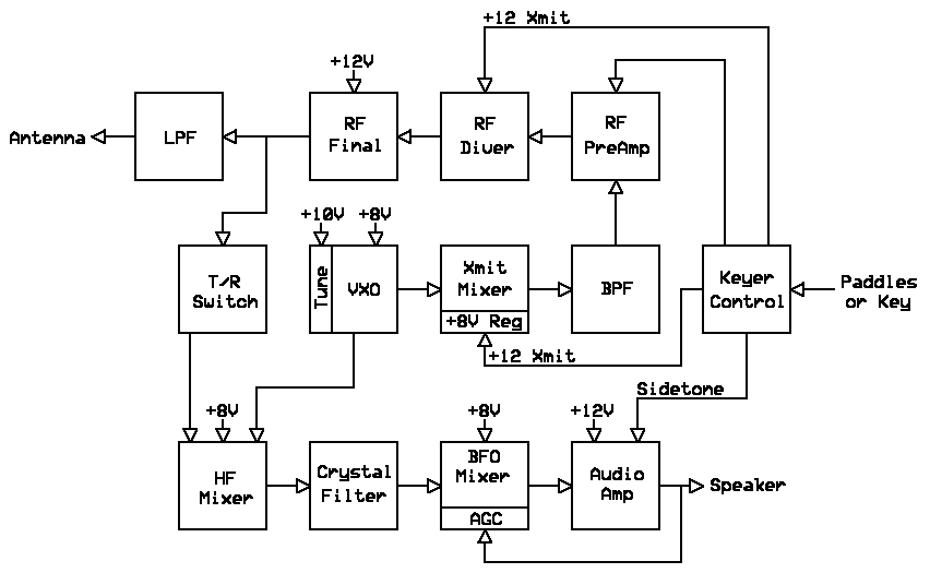
Block Diagram
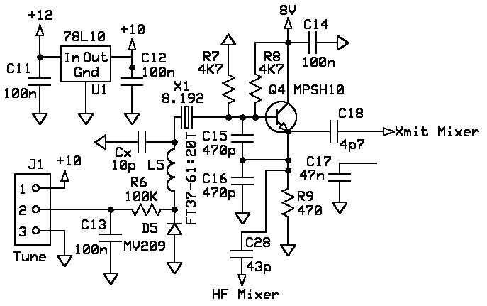
Voltage Controlled Crystal Oscillator (VCXO)
Receiver Section
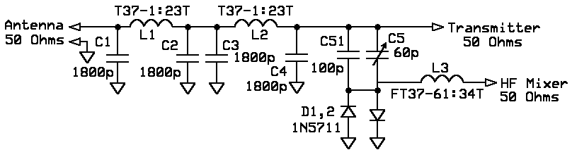
Low Pass Filter
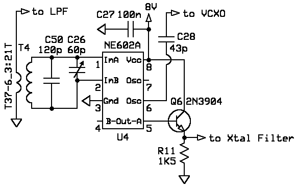
First Mixer
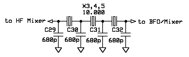
Crystal Filter
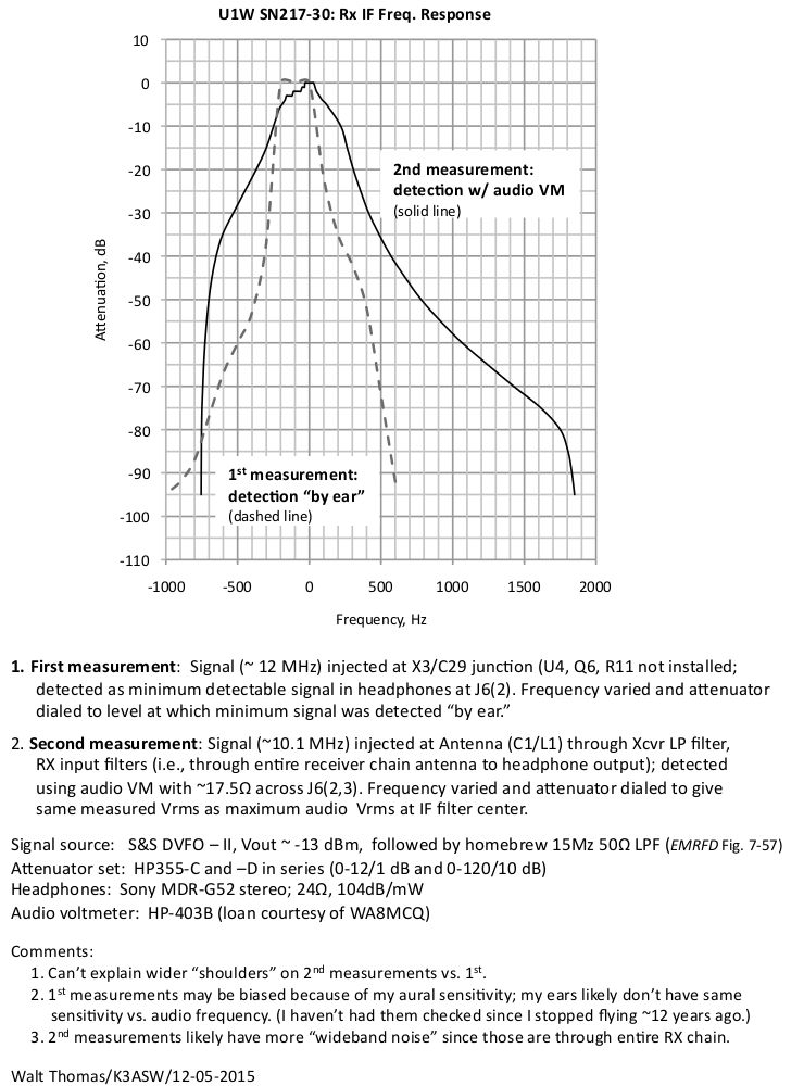
Frequency Response (by K3ASW)
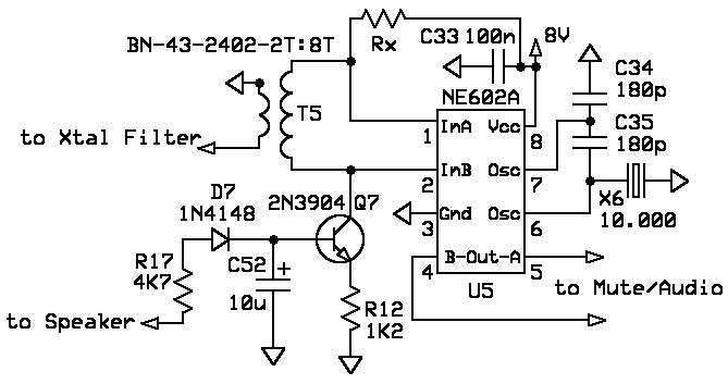
Audio Detector Mixer (BFO) with AGC
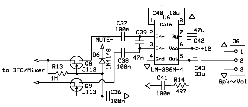
Audio Amplifier with Mute
Transmitter Section
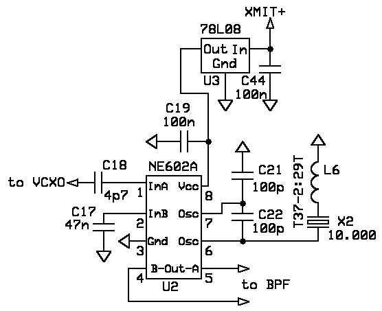
Transmit Carrier Oscillator Mixer
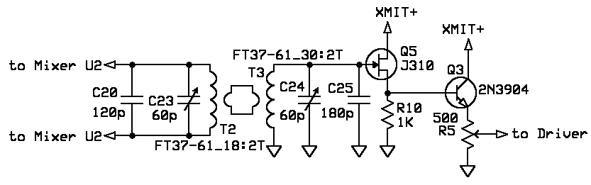
Transmit Band Pass Filter and Preamps
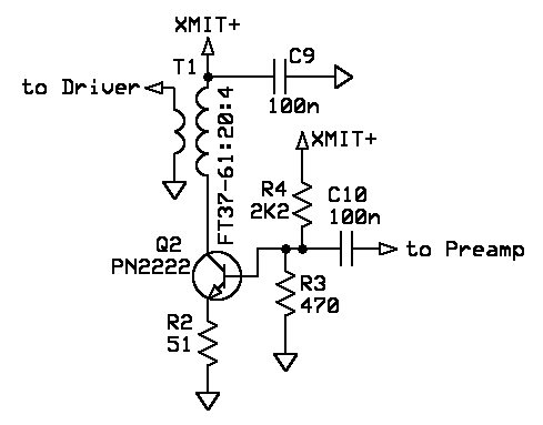
Transmit Driver
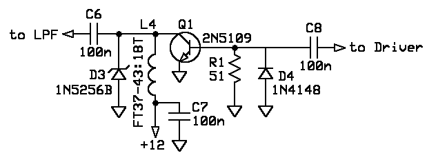
Transmit Final Amplifier
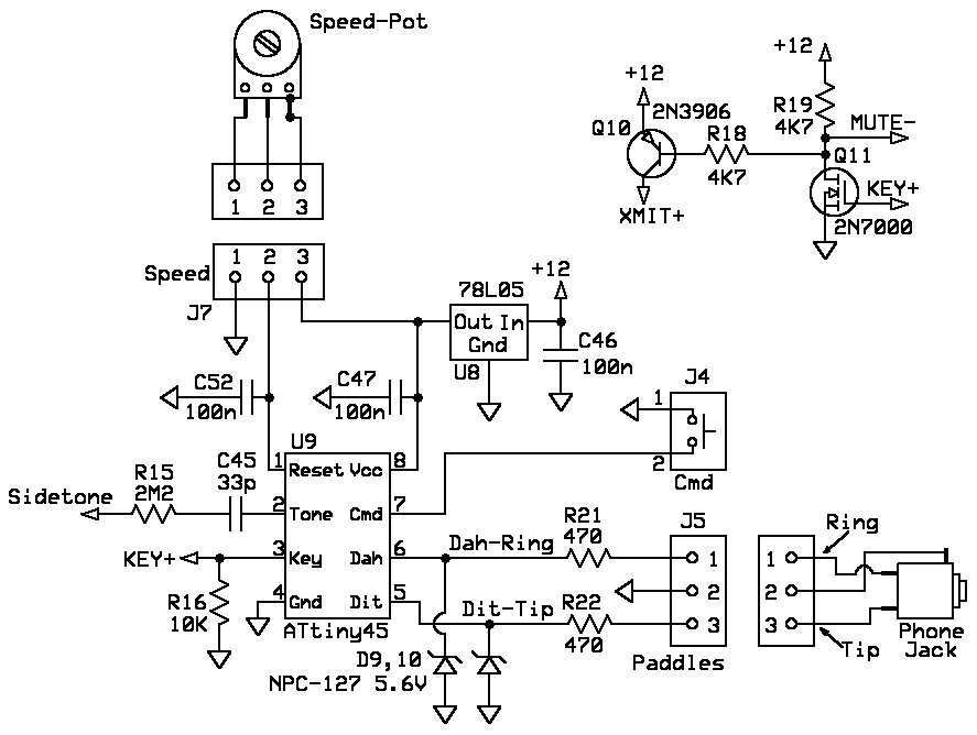
Keyer and QSK Operation
Schematic
Printed Circuit Board